Showing posts with label 8087. Show all posts

Die analysis of the 8087 math coprocessor's fast bit shifter

Floating-point numbers are very useful for scientific programming, but early microprocessors only supported integers directly.1 Although floating-point was common in mainframes back in the 1950s and 1960s, it wasn't until 1980 that Intel introduced the 8087 floating-point coprocessor for microcomputers.2 Adding this chip to a microcomputer such as the IBM PC made floating-point operations up to 100 times faster. This was a huge benefit for applications such as AutoCAD, spreadsheets, or flight simulators.3 The downside was the 8087 chip cost hundreds of dollars.4

It's hard to implement floating-point operations so they are computed quickly and accurately. Problems can arise from overflow, rounding, transcendental operations, and numerous edge cases. Prior to the 8087, each manufacturer had their own incompatible ad hoc implementation of floating point. Intel, however, enlisted numerical analysis expert William Kahan to design accurate floating point based on rigorous principles.5 The result was the floating-point architecture of the 8087. This became the IEEE 754 standard used in almost all modern computers, so I consider the 8087 one of the most influential chips ever designed.

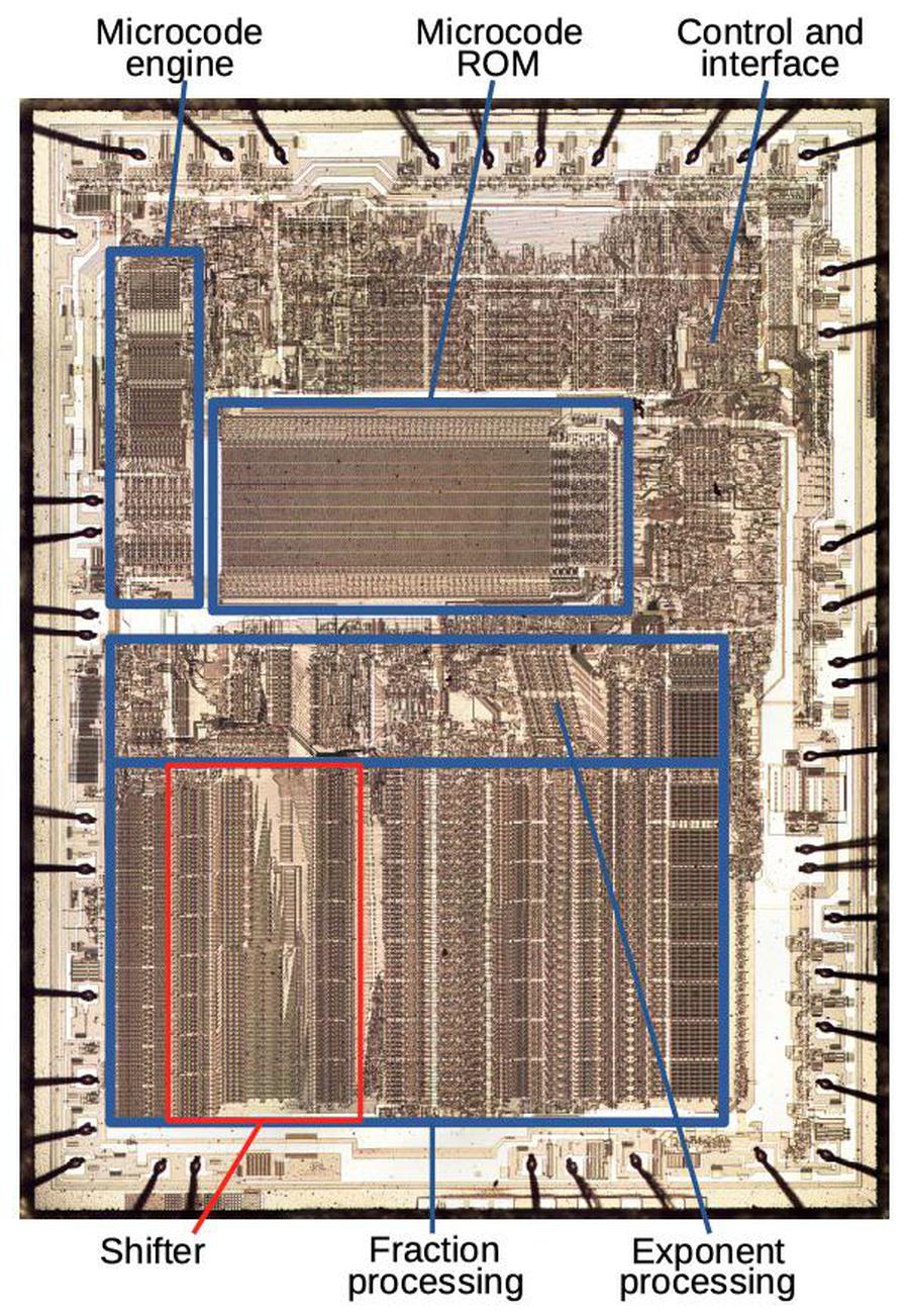
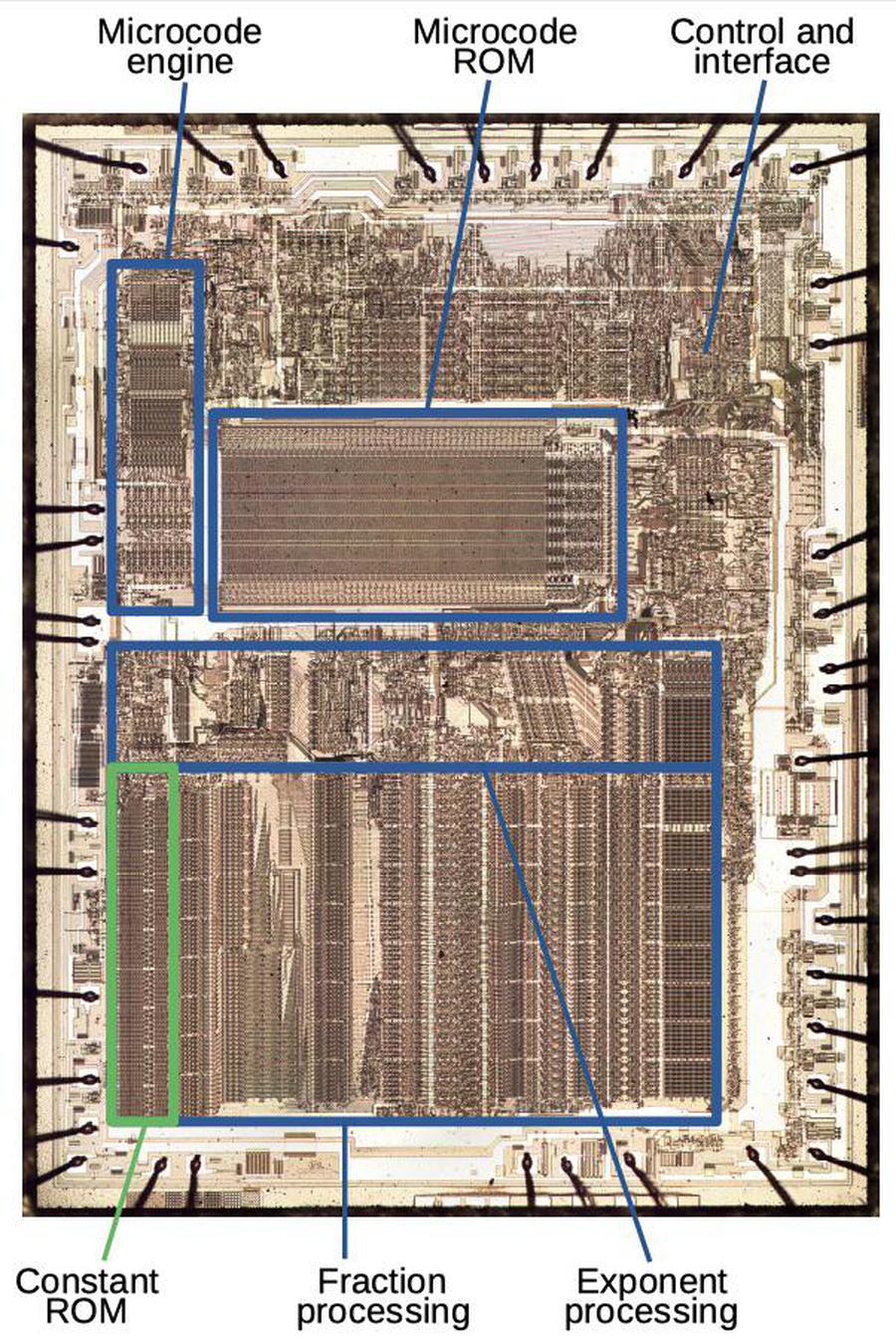
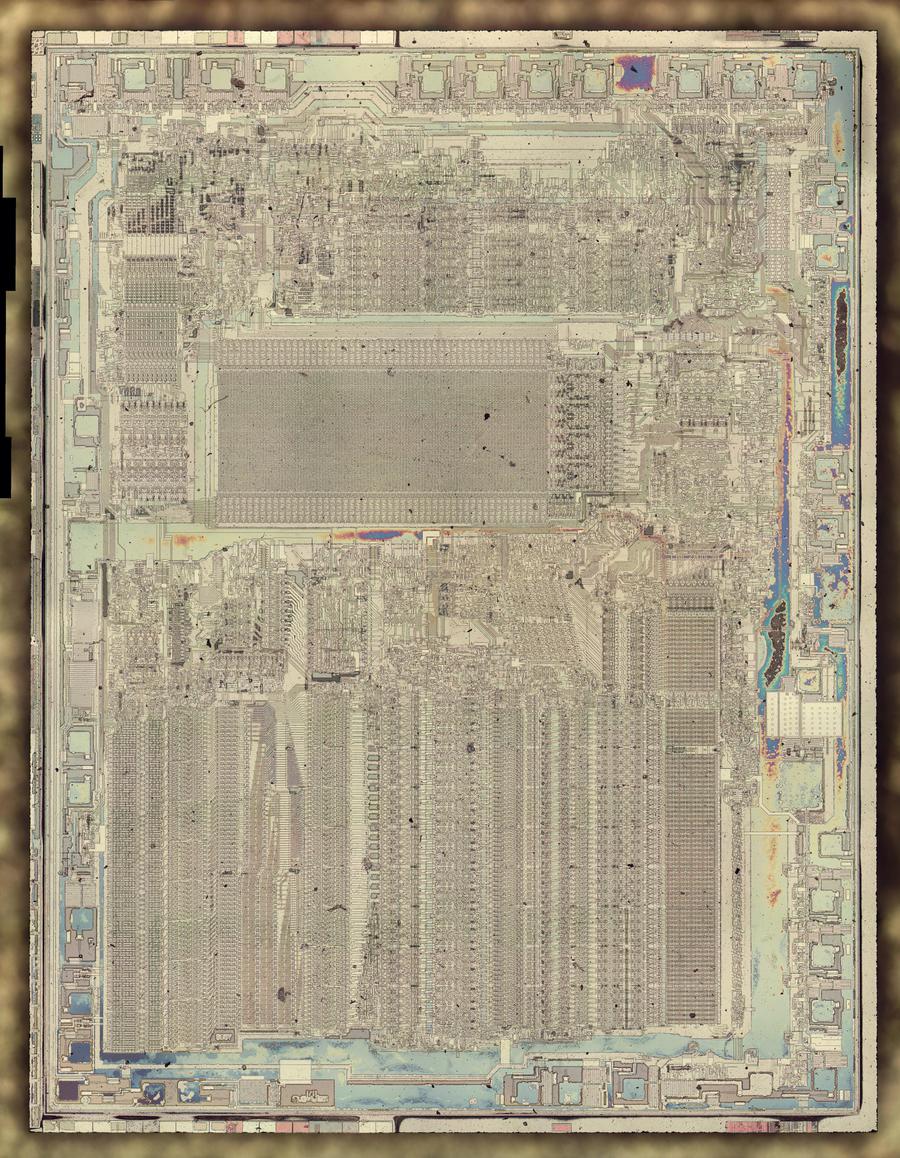
Die of the Intel 8087 floating point unit chip, with main functional blocks labeled. The die is 5mm×6mm. The shifter is outlined in red. Click for a larger image.

Die of the Intel 8087 floating point unit chip, with main functional blocks labeled. The die is 5mm×6mm. The shifter is outlined in red. Click for a larger image.

To explore how the 8087 works, I opened up an 8087 chip and took photos of the silicon die with a microscope. Containing 40,000 transistors, the 8087 pushed chip manufacturing to the limit; in comparison, the companion 8086 microprocessor only had 29,000 transistors. To make the chip possible, Intel developed new techniques. In this article, I focus on the high-speed binary shifter (outlined in red above). The shifter takes up a large fraction of the chip's area, so minimizing its area was vital to making the 8087 possible.

A floating-point number consists of a fraction (also called significand or mantissa), an exponent, and a sign bit. (These are expressed in binary, but for a base-10 analogy, the number 6.02×10²³ has 6.02 as the fraction and 23 as the exponent.) The circuitry to process the fraction is at the bottom of the die photo. From left to right, the fraction circuitry consists of a constant ROM, a shifter (highlighted), adder/subtracters, and the register stack. The exponent processing circuitry is in the middle of the chip. Above it, the microcode engine and ROM control the chip.

The shifter

The role of the shifter is to shift binary numbers left or right, a task with several critical roles in floating-point operations. When two floating-point numbers are added or subtracted, the numbers must be shifted so the binary points line up. (The binary point is like the decimal point, but for a binary number.) The 8087's transcendental instructions are built around shift and add operations, using an algorithm called CORDIC. The shifter is also used to assemble a floating-point number from 16-bit chunks read from memory.8

Since shifts are so essential to performance, the 8087 uses a "barrel shifter", which can shift a number by any number of bits in a single step.6 Intel used a two-stage shifter design that kept its size manageable while still providing high performance. The first stage shifts the value by 0 to 7 bits, while the second stage shifts by 0 to 7 bytes. In combination, the two stages shift a value by any amount from 0 to 63 bits.

The bit shifter

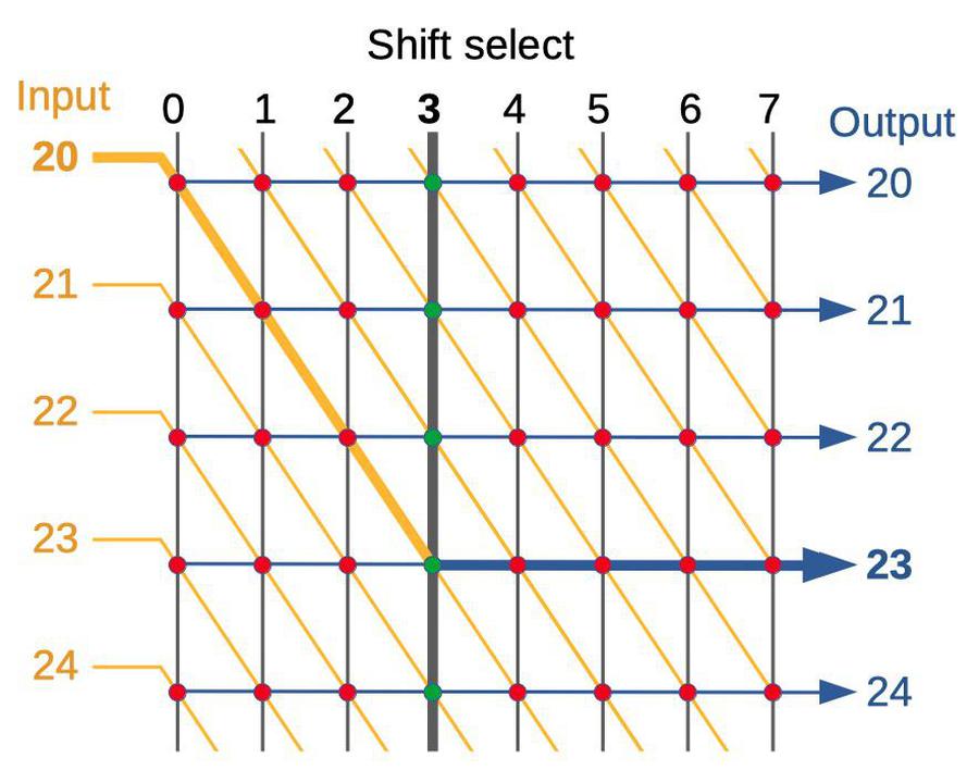
I'll start by describing the bit shifter, which performs a shift of 0 to 7 bit positions. The diagram below outlines the structure of the bit shifter, showing five of the inputs and outputs; the full shifter supports 68 bits.7 The concept is that by activating a particular column, the input is shifted by the desired amount. Each circle indicates a transistor that can act as a switch between an input line and an output line. The vertical select lines are used to activate the desired transistors. Each input line is connected diagonally to eight transistors, allowing it to be directed to one of eight outputs. For example, the diagram shows shift select line 3 activated, turning on the associated transistors (green). The highlighted input 20 (orange) is directed to output 23 (blue). Similarly, the other inputs are connected to the corresponding outputs, yielding a shift by 3. By activating a different shift select line, the input will be shifted by a different amount between 0 and 7 bits.

Structure of the bit shifter. By energizing a shift select line, the inputs are connected to outputs with the desired bit shift.

Structure of the bit shifter. By energizing a shift select line, the inputs are connected to outputs with the desired bit shift.

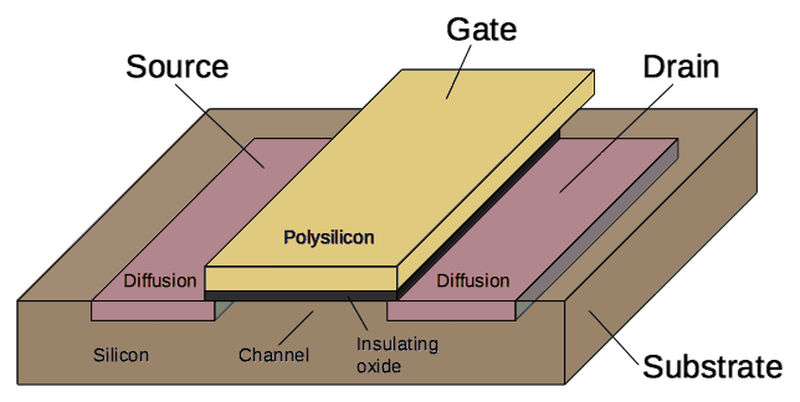
To explain the internal construction of the shifter, I'll start by describing the NMOS transistors used in the 8087 chip. Transistors are built by doping areas of the silicon substrate with impurities to create "diffusion" regions with different electrical properties. The transistor can be considered a switch, controlling the flow of current between two regions called the source and drain. The transistor is activated by the gate, made of a special type of silicon called polysilicon, layered above the substrate silicon. Applying voltage to the gate lets current flow between the source and drain, which is otherwise blocked. Transistors are wired together by a metal layer on top, building a complex integrated circuit.

Structure of a MOSFET as implemented in an integrated circuit.

Structure of a MOSFET as implemented in an integrated circuit.

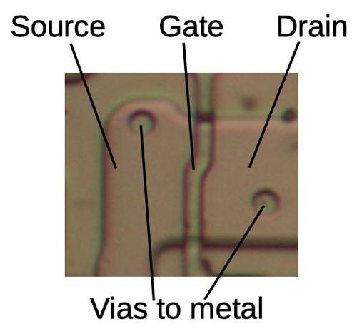
The photo below shows a transistor in the 8087 as it appears under the microscope. Its structure matches the diagram above, although its shape is more complex. The source, gate, and drain all continue out of the photo, connected to other transistors. In addition, wiring in the metal layer is connected to the silicon at the circular vias. (The metal layer was removed with acid for this photo.)

An NMOS transistor in the 8087 chip, as seen under the microscope.

An NMOS transistor in the 8087 chip, as seen under the microscope.

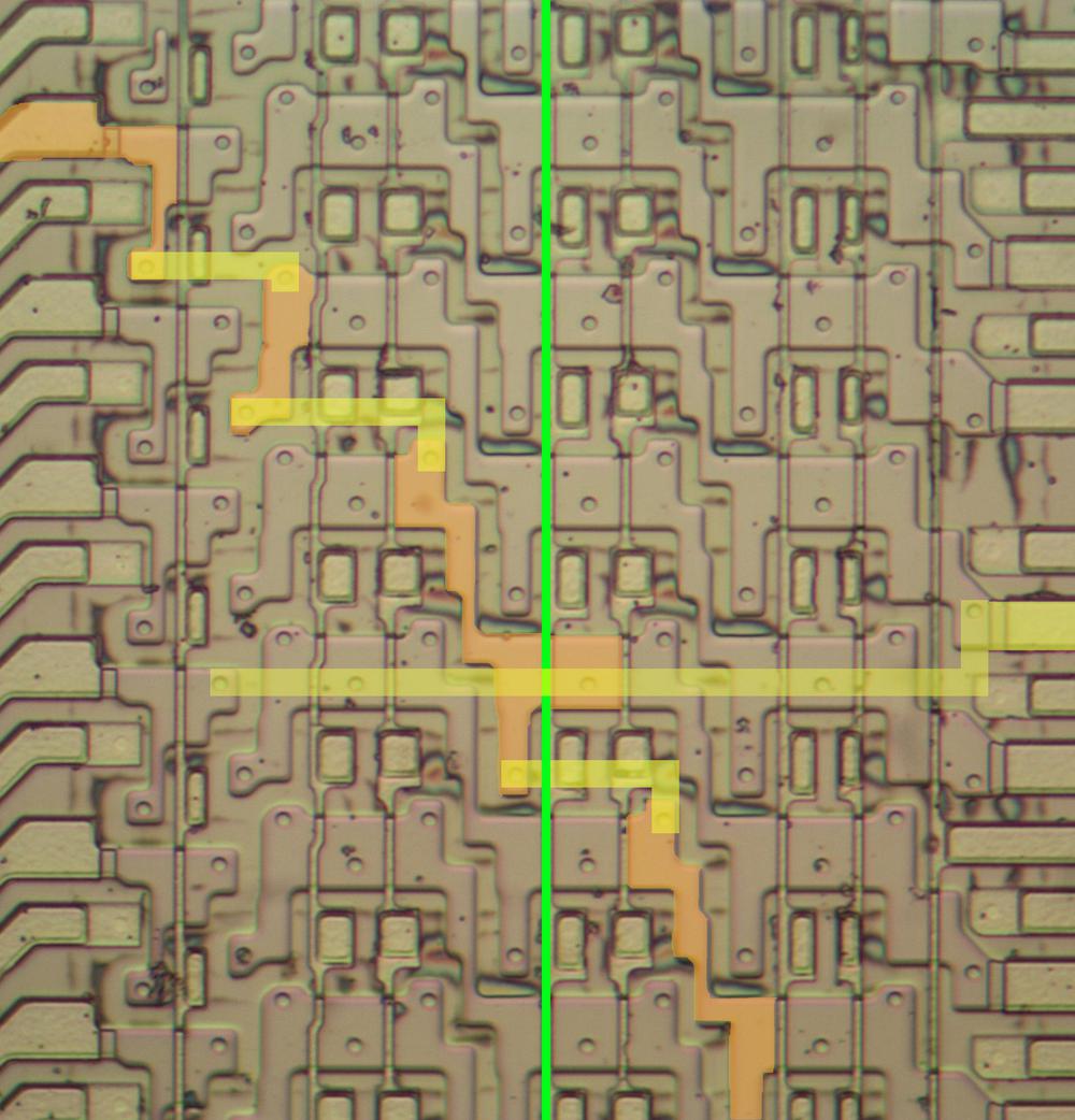
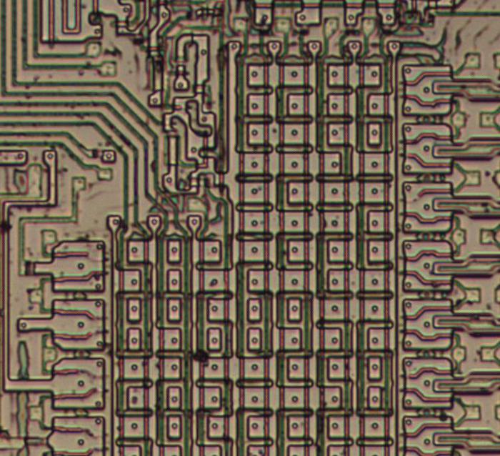
Zooming out, the diagram below shows part of the bit shifter as implemented on the chip. About 48 transistors, similar to the one above, are in this photo. The orange and yellow diagonal corresponds to one of the inputs: the orange regions show transistors connected through the silicon, while the yellow lines show connections in the metal layer. (The metal layer is used to jump over the polysilicon select lines.) The green highlight shows the polysilicon line for shift-by-three. In the center, this polysilicon gate line turns on a transistor, connecting the input to the long yellow output line, shifting the highlighted input by three positions. (The other non-highlighted inputs are shifted similarly.) Thus, this circuit implements the shifter as described at the beginning of the section. The photo shows six of the 68 inputs, so the complete shifter is much taller.

Closeup of the silicon circuitry for the bit shifter. The path of one signal is shown, as controlled by the shift-by-three control (green).

Closeup of the silicon circuitry for the bit shifter. The path of one signal is shown, as controlled by the shift-by-three control (green).

The byte shifter

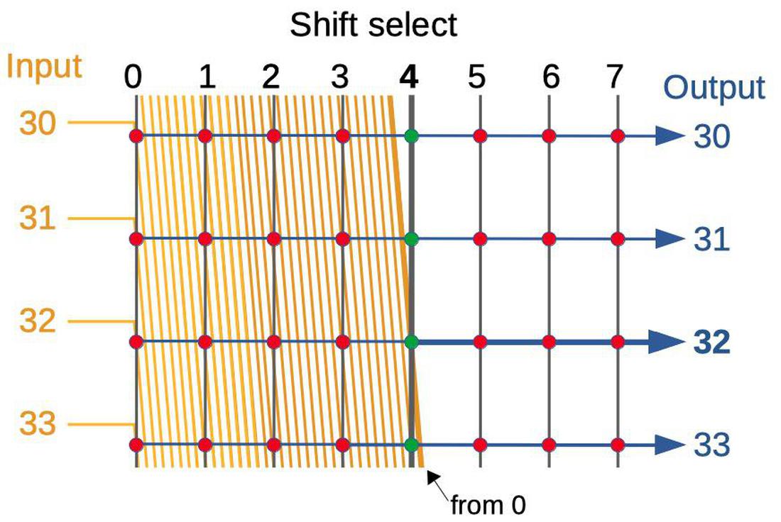
The byte shifter shifts its inputs by multiples of eight bits, rather than one bit. Its design is similar to the bit shifter, except each input connects to every eighth output. For instance, input 20 connects to outputs 20, 28, 36, and so forth, shifting by bytes. As a result, the diagonal connections are steep and packed tightly, with eight lines between each switch. In the diagram below, the line for shift-by-four is selected, with the connection from input 0 to output 32 highlighted. Note the lack of wires in the right half of the diagram because any bit shifted from beyond input 0 becomes zeroed. For instance, when shifting left by 4 bytes, low-order bits 31 and below become zero.

The structure of the byte shifter.

The structure of the byte shifter.

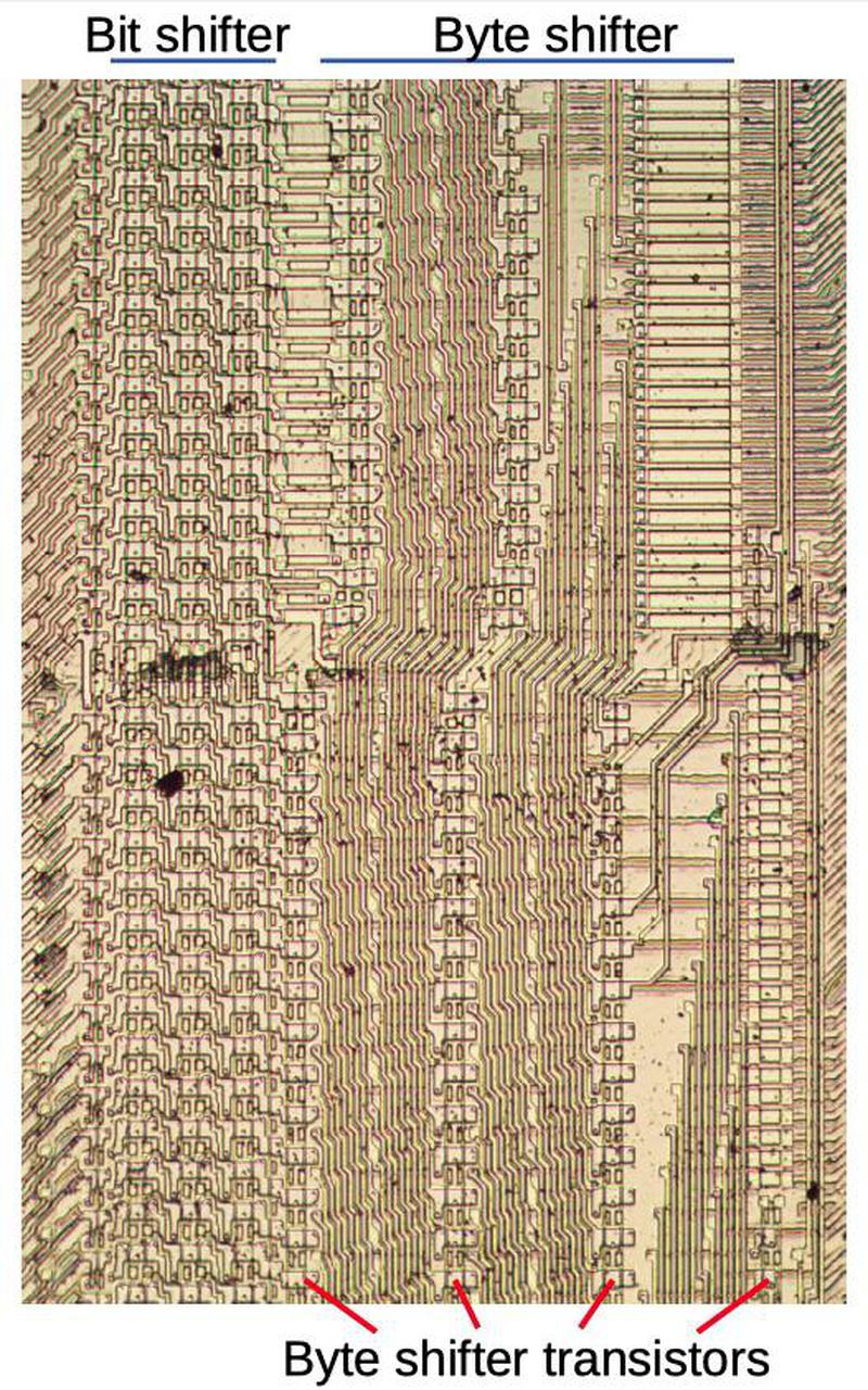
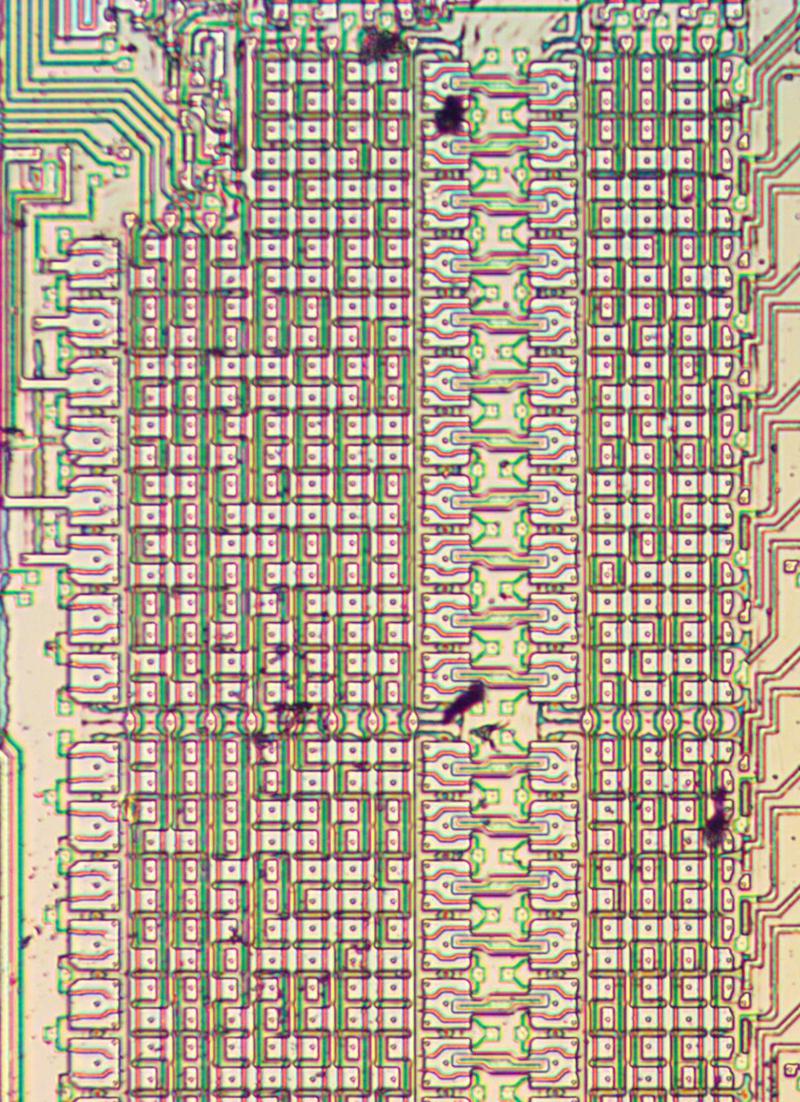
The die photo below shows part of the bit shifter and the byte shifter. This photo is zoomed-out to show the overall structure; individual transistors are barely visible. The bit shifter's area is densely packed with transistors, but the byte shifter consists mostly of wiring, with columns of transistors in between.9 Also note that the byte shifter is partially empty at the top, filling in with more wiring towards the bottom. The wiring layout isn't as orderly as in the diagram above, but is arranged for maximum efficiency.

The bit shifter and byte shifter in the 8087 chip.

The bit shifter and byte shifter in the 8087 chip.

The bidirectional drivers

So far, the bit and byte shifters only shift bits in one direction.11 However, bits need to be shifted in both directions. One of the key innovations of the 8087's shifter is its bidirectional design: data can be passed through the shifter in reverse to shift bits the opposite direction. This is possible because the shifter is constructed with pass transistors, not logic gates. Pass transistor logic uses transistors as switches that pass or block signals, so signals can travel in either direction. (In contrast, regular logic gates such as NOR gates have specific inputs and outputs.)

Special driver circuitry on the left and right sides of the shifter allows the shifter to operate in either direction. To send data from left to right, the left-hand driver reads data from the fraction bus and sends it into the shifter. The right-hand driver circuit receives this shifted data, latches it temporarily, and then writes it back to the fraction bus. To send data in the opposite direction, the driver circuits reverse roles: the right-hand driver sends data from the fraction bus into the shifter while the left-hand circuit receives the shifted data.10

The multiplexer / decoders

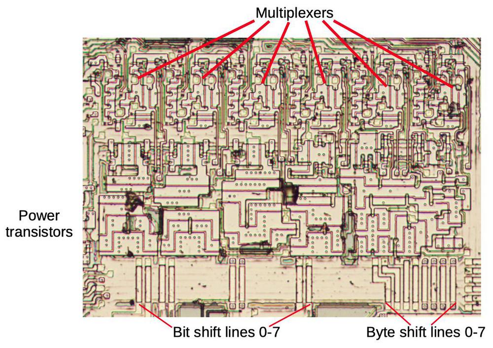
The final feature I'll describe is the circuitry that controlled the shifter. Three different sources control how many positions to shift. First, the microcode engine can specify the number directly. Second, the number can come from a loop counter; this is used as part of the CORDIC transcendental algorithms. Finally, the number can come from a leading zero counter; this allows numbers to be normalized by eliminating leading zeroes through shifting. Each of these sources provides a 6-bit shift number; the six multiplexers each select one bit from the desired source.12

The multiplexer/decoder circuitry.

The multiplexer/decoder circuitry.

Next, decoders activate one of eight bit-shift lines and one of eight byte-shift lines to control the appropriate pass transistors in the shifter. (Each decoder takes a 3-bit input and activates one of 8 output lines.) Because each decoder line controls a large column of pass transistors in the shifter, the decoder uses relatively large power transistors.13 At the bottom, the 16 control lines exit the circuitry.

Conclusion

The 8087 is a complex chip with many functional units. However, by examining the die closely, the circuits of the 8087 can be understood. This blog post described the 8087's fast barrel shifter, capable of shifting by up to 63 bits at a time.14 Intel received a patent on this innovative programmable bidirectional shifter.

The shifter was just one of the features that let the 8087 compute floating-point operations much faster than the 8086 processor could. The 8087 operates on 80 bits at a time instead of 16. The 8087 has 80-bit wide registers, reducing memory accesses during computations. The 8087 stores constants for transcendental operations in a ROM, also avoiding memory accesses. Hardware in the 8087 checked for NaN, underflow, overflow, etc., avoiding slow checks in code. The 8087's hardware made multiplication and division faster. I don't know the relative contributions of these factors, but in combination, they improved floating-point performance dramatically, by up to a factor of 100.

The benefits of floating point hardware are so great that Intel started integrating the floating-point unit into the processor with the 80486 (1989). Now, most processors include a floating-point unit and the expense of purchasing a separate floating-point coprocessor is a thing of the past.

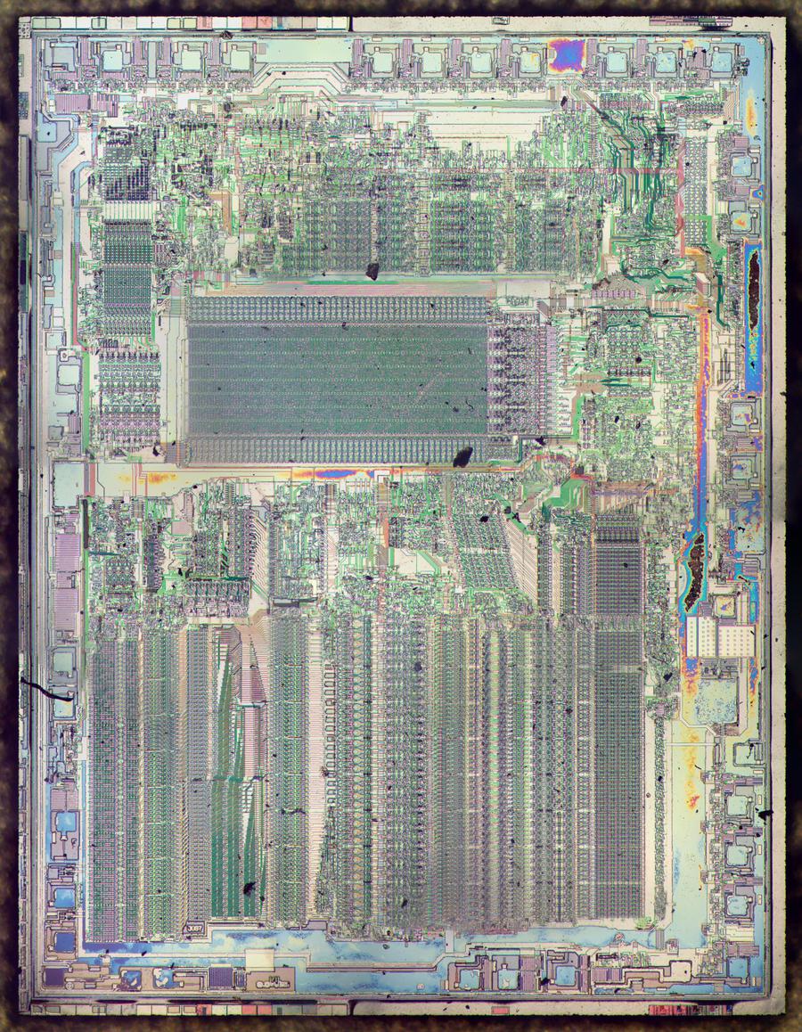
Die photo of the 8087 with the metal layer removed. The colors are due to some of the oxide layer remaining. Click for a larger image.

Die photo of the 8087 with the metal layer removed. The colors are due to some of the oxide layer remaining. Click for a larger image.

For more information on the 8087, see my other articles: Extracting ROM constants from the 8087, The two-bit-per-transistor ROM and The substrate bias generator. I announce my latest blog posts on Twitter, so follow me @kenshirriff for future articles. I also have an RSS feed.

Notes and references

  1. Even without floating-point hardware, early microcomputers could perform floating-point operations. The operations would be broken down into many integer operations, manipulating the exponent and fraction as necessary. In other words, floating-point support didn't make floating-point operations possible, it just made them much faster. (Another way to represent non-integers is fixed-point numbers, which have a fixed number of digits after the decimal. Fixed-point numbers are simpler than floating-point, but can't represent as large a range.) 

  2. The 8087 wasn't the first floating-point chip. National Semiconductor introduced the MM57109 Number Cruncher Unit (that is the real name) in 1977. It was essentially a repackaged 12-digit scientific calculator chip, operating on binary-coded decimal values with values entered in Reverse Polish Notation. This chip was absurdly slow; a tangent, for instance, could take over a second. AMD introduced their floating-point chip, the Am9511, in 1978 (details). This chip supported 32-bit floating-point numbers and took up to 1.4 milliseconds for a tangent. (Intel ended up licensing the Am9511 from AMD and selling it as the 8231.) A 10-MHz 8087 in comparison, could do a tangent in 54 microseconds, operating on an 80-bit floating-point number. Thus, the 8087's performance and accuracy were far superior to previous chips. 

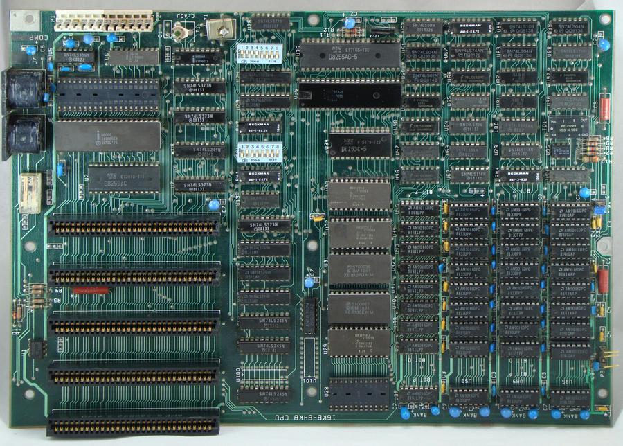
  3. The original IBM PC (1981) had an empty socket on its motherboard for adding an 8087 coprocessor. a huge benefit for applications such as AutoCAD. The large empty socket is visible in the upper left below, above the 8088 microprocessor. A list of applications with support for the 8087 is here.

    Motherboard of the original IBM PC (1981).
Photo from Wikimedia, CC BY-SA 3.0.

    Motherboard of the original IBM PC (1981). Photo from Wikimedia, CC BY-SA 3.0.


  4. I couldn't find the original price for the 8087, but it was expensive. At first, Intel only sold the 8087 as a matched and tested pair with an 8088, due to timing flakiness with the 8087. By 1982, Intel dropped the price of the 8087 to $230, equivalent to about $500 in current dollars. Compared to today's open-source world, it seems strange that customers also had to pay for software support: using the 8087 with the BASIC language cost another $150, while Intel's 8087 development library was $1250. 

  5. The designers of the 8087 commented on the guidance offered by Professor Kahan: "We did not do as well as he wanted, but we did better than he expected." Kahan later received a Turing Award for his work on floating point.  

  6. Processors often include a variety of shift instructions, including rotate operations that shift bits from one end of the word to the other. The 8087 only performs straight shifts, not rotates. 

  7. The shifter handles the 8087's 64-bit fraction, along with three extra bits for rounding accuracy, so it supports 67 bits. Unless I miscounted, the shifter also has an extra bit in the most significant position, making it 68 bits wide. 

  8. Multiplication and division make heavy use of shifting; multiplication is performed by shifts and adds, while division uses shifts and subtracts. However, the 8087 does not use the general-purpose shifter for these operations, but has specialized shifters optimized for these operations. 

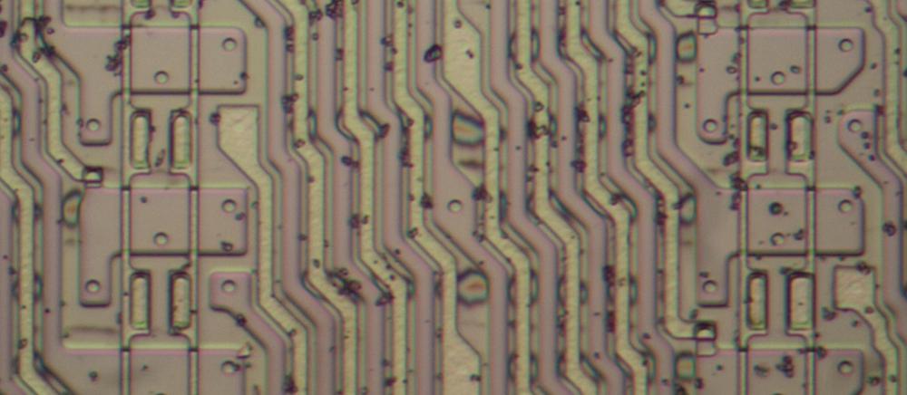
  9. In order to pack the wiring as close together as possible, the shifter alternated wires of diffused silicon and wires of polysilicon. In the photo below, the diffused silicon wires are pinkish, while the polysilicon is yellowish. The 8087 was built with Intel's HMOS III process, which required a 4µm spacing for polysilicon and 5µm for diffusion, probably due to the resolution of the photolithography practice. However, the spacing between a diffusion line and a polysilicon line could be much smaller, probably because they were created with separate masks and were on separate layers. Thus, alternating diffusion and polysilicon lines could be packed together tightly, saving space.

    Wiring in the byte shifter consists of alternating, tightly-packed silicon and polysilicon lines. The large rectangles on either side are pairs of transistors, controlled by vertical polysilicon lines.

    Wiring in the byte shifter consists of alternating, tightly-packed silicon and polysilicon lines. The large rectangles on either side are pairs of transistors, controlled by vertical polysilicon lines.

  10. The driver circuitry has a few subtleties. Instead of sending data directly into the shifter, bits are transferred in two steps. First, the shifter lines are pre-charged to a high level. Then, any 1-bit inputs cause the corresponding shifter lines to be pulled low. In other words, the shifter lines are active-low, with a low voltage representing a 1. Since any unused outputs keep their high voltage (a 0 bit), 0 bits are shifted into low bit positions automatically. I think the pre-charge technique also was a better match for NMOS circuitry, which was better at pulling a signal low than pulling it high, so pre-charging the lines helped performance, especially given their relatively high capacitance. The latch between the shifter and the fraction bus prevents an unwanted cycle with the shifted data immediately flowing back into the shifter and getting re-shifted. 

  11. This footnote will clarify the physical shift versus the logical shift. On the die, the fraction circuitry is arranged with the most-significant bit at the bottom. Passing data through the shifter from left to right shifts bits physically downward. This corresponds to a left-shift of a binary number, moving bits to a higher position. In the opposite direction, passing data through the shifter from right to left performs a right-shift of the data. 

  12. The left/right direction also needs to be selected from one of the three shift sources, but I haven't located the circuitry for that yet. 

  13. Each decoder essentially consists of eight NOR gates: seven will be pulled low and only the one with all inputs low will be high. However, it's not implemented as a straightforward logic gate. Instead, all outputs are precharged high, and then the seven undesired outputs are pulled low. This sort of dynamic precharge logic is still used in modern circuits; see the book Synchronous Precharge Logic. The multiplexers are also implemented with precharge logic. 

  14. Intel's x86 processors didn't include a barrel shifter until the 80386 (1985), which provided a 64-bit barrel shifter. Before that, the 8086 and descendants shifted one bit at a time, so shifts by many bit positions were much slower. 

Extracting ROM constants from the 8087 math coprocessor's die

Intel introduced the 8087 chip in 1980 to improve floating-point performance on the 8086 and 8088 processors, and it was used with the original IBM PC. Since early microprocessors operated only on integers, arithmetic with floating-point numbers was slow and transcendental operations such as arctangent or logarithms were even worse. Adding the 8087 co-processor chip to a system made floating-point operations up to 100 times faster.

I opened up an 8087 chip and took photos with a microscope. The photo below shows the chip's tiny silicon die. Around the edges of the chip, tiny bond wires connect the chip to the 40 external pins. The labels show the main functional blocks, based on my reverse engineering. By examining the chip closely, various constants can be read out of the chip's ROM, numbers such as pi that the chip uses in its calculations.

Die of the Intel 8087 floating point unit chip, with main functional blocks labeled. The constant ROM is outlined in green. Click for a larger image.

Die of the Intel 8087 floating point unit chip, with main functional blocks labeled. The constant ROM is outlined in green. Click for a larger image.

The top half of the chip contains the control circuitry. Performing a floating-point instruction might require 1000 steps; the 8087 used microcode to specify these steps. The die photo above shows the "engine" that ran the microcode program; it is basically a simple CPU. Next to it is the large ROM that holds the microcode.

The bottom half of the die holds the circuitry that processes floating-point numbers. A floating-point number consists of a fraction (also called significand or mantissa), an exponent, and a sign bit. (For a base-10 analogy, in the number 6.02×10²³, 6.02 is the fraction and 23 is the exponent.) The chip has separate circuitry to process the fraction and the exponent in parallel. The fraction processing circuitry supports 67-bit values, a 64-bit fraction with three extra bits for accuracy. From left to right, the fraction circuitry consists of a constant ROM, a shifter, adder/subtracters, and the register stack. The constant ROM (highlighted in green) is the subject of this post.

The 8087 operated as a co-processor with the 8086 processor. When the 8086 encountered a special floating-point instruction, the processor ignored it and let the 8087 execute the instruction in parallel.1 I won't explain in detail how the 8087 works internally, but as an overview, floating-point operations are implemented using integer adds/subtracts and shifts. To add or subtract two floating-point numbers, the 8087 shifts the numbers until the binary points (i.e. the decimal points but in binary) line up, and then adds or subtracts the fraction. Multiplication, division, and square root are performed through repeated shifts and adds or subtracts. Transcendental operations (tan, arctan, log, power) use CORDIC algorithms, which use shifts and adds of special constants for efficient computation.

Implementation of the ROM

This post describes the ROM that holds constants (not to be confused with the larger, four-level microcode ROM.2) The constant ROM holds the constants (such as pi, ln(2), and sqrt(2)) that the 8087 needs for its computations. The photo below shows part of the constant ROM. The metal layer has been removed to show the silicon underneath. The pinkish regions are silicon doped to have different properties, while the reddish and greenish lines are polysilicon, a special type of silicon wiring layered on top. Note the regular grid structure of the ROM. The ROM consists of two columns of transistors, holding the bits. To explain how the ROM works, I'll start by explaining how a transistor works.

Part of the constant ROM, with the metal layer removed. The three columns of larger transistors are used to select between rows.

Part of the constant ROM, with the metal layer removed. The three columns of larger transistors are used to select between rows.

High-density integrated circuits in the 1970s were usually built from a type of transistor known as NMOS. (Modern computers are built from CMOS, which consists of NMOS transistors along with opposite-polarity PMOS transistors.) The diagram below shows the structure of an NMOS transistor. An integrated circuit is constructed from a silicon substrate, with transistors built on it. Regions of the silicon are doped with impurities to create "diffusion" regions with desired electrical properties. The transistor can be viewed as a switch, allowing current to flow between two diffusion regions called the source and drain. The transistor is controlled by the gate, made of a special type of silicon called polysilicon. Applying voltage to the gate lets current flow between the source and drain, which is otherwise blocked. The die of the 8087 is fairly complex, with about 40,000 of these transistors.3

Structure of a MOSFET as implemented in an integrated circuit.

Structure of a MOSFET as implemented in an integrated circuit.

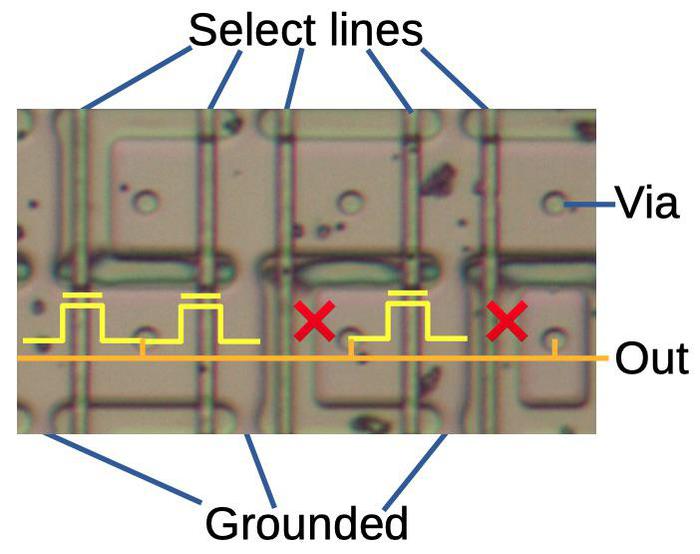
Zooming in on the ROM shows the individual transistors. The pinkish regions are the doped silicon, forming transistor sources and drains. The vertical polysilicon select lines form the gates of the transistors. The indicated silicon regions are connected to ground, pulling one side of each transistor low. The circles are connections called vias between the silicon and the metal lines above. (The metal lines have been removed; the orange line shows the position of one.)

A portion of the constant ROM. Each select line selects a particular constant. Transistors are indicated by the yellow symbols. An X indicates a missing transistor, corresponding to a 0 bit. The orange line indicates the position of a metal wire. (The metal layer was dissolved for this picture.)

A portion of the constant ROM. Each select line selects a particular constant. Transistors are indicated by the yellow symbols. An X indicates a missing transistor, corresponding to a 0 bit. The orange line indicates the position of a metal wire. (The metal layer was dissolved for this picture.)

The important feature of the ROM is that some of the transistors are missing, the first one in the upper row, and two marked with X in the lower row. Bits are programmed into the ROM by changing the silicon doping pattern, creating transistors or leaving insulating regions. Each transistor or missing transistor represents one bit. When a select line is activated, all the transistors in that column will turn on, pulling the corresponding output lines low. But if the transistor is missing from a selected position, the corresponding output line will remain high. Thus, a value is read from the ROM by activating a select line, reading that ROM value onto the output lines.

Contents of the ROM

The constant ROM has 134 rows of 21 columns.5 Under a microscope, the bit pattern of the ROM is visible and can be extracted.4 How to interpret the raw bits is not obvious, though. The first question is if a transistor (versus a gap) indicates a 0 or a 1. (It turns out that a transistor indicates a 1 bit.) The next issue is how to map the 134×21 grid of bits into values.6

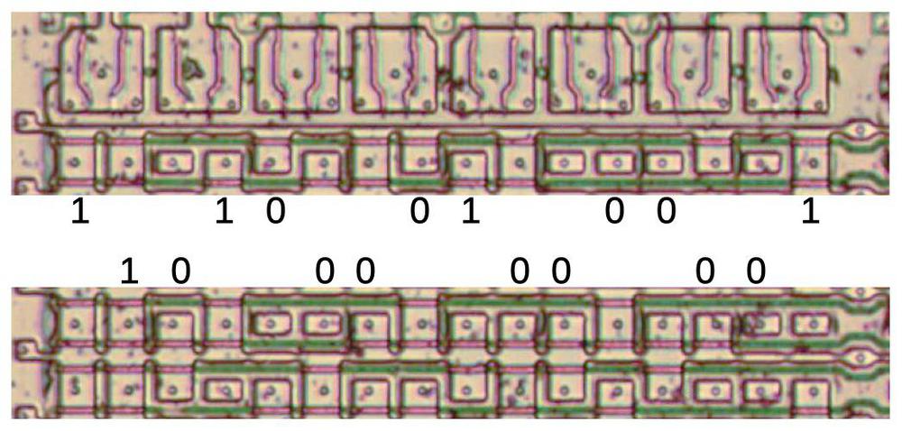
The chip's data path consists of 67 horizontal rows, so it seemed pretty clear that the 134 rows in the ROM corresponded to two sets of 67-bit constants. I extracted one set of constants for the odd rows and one for the even rows, but the values didn't make any sense. After more thought, I determined that the rows do not alternate but are arranged in a repeating "ABBA" pattern.7 Using this pattern yielded a bunch of recognizable constants, including pi and 1. Bits from those constants are shown in the diagram below. (In this photo, a 1 bit appears as a green stripe, while a 0 bit appears as a red stripe.) In binary, pi is 11.001001... and this value is visible in the upper labeled bits. The bottom value is the constant 1.8

Bit values labeled in the constant ROM. The top bits are the first part of pi, while the lower bits are the constant 1, This diagram has been rotated 90 degrees compared to the other diagrams. The unlabeled bits form other constants.

Bit values labeled in the constant ROM. The top bits are the first part of pi, while the lower bits are the constant 1, This diagram has been rotated 90 degrees compared to the other diagrams. The unlabeled bits form other constants.

The next difficulty in interpretation is that this ROM holds just the fractional parts of the numbers, not the exponents. (I haven't found the separate exponent ROM yet.) I experimented with various exponents until I got values that were sensible numbers. Some were straightforward: for instance, the constant 1.204120 yielded log10(2) when the exponent 2-2 was used. Others were harder,9 such as 1.734723. Eventually, I figured out that 1.734723×259 is 1018.10

The complete table of constants is in the footnotes.11 Physically, the constants are arranged in three groups. The first group is values that the user can load (1, pi, log210, log2e, log102, and ln 2)12 along with values used internally (1018, ln(2)/3, 3*log2(e), log2(e), and sqrt(2)). The second group is sixteen arctan constants, and the third is fourteen log2 constants. The last two groups of constants are used to compute transcendental functions using the CORDIC algorithm, which I will discuss next.

The CORDIC algorithms

The constants in the ROM reveal some details about the algorithms used by the 8087. The ROM contains 16 arctangent values, the arctans of 2-n. It also contains 14 log values, the base-2 logs of (1+2-n). These may seem like unusual values, but they are used in an efficient algorithm called CORDIC, which was invented in 1958.

The basic idea of CORDIC is to compute tangent and arctangent by breaking down an angle into smaller angles, and rotating a vector by these angles. The trick is that by carefully choosing the smaller angles, each rotation can be computed with efficient shifts and adds instead of trig functions. Specifically, suppose we want to find tan(z). We can break z into a sum of smaller angles: z ≈ {atan(2-1) or 0} + {atan(2-2) or 0} + {atan(2-3) or 0} + ... + {atan(2-16) or 0}. Now, rotating a vector by, say atan(2-2), can be done by multiplying by 2-2 and adding. The key thing is that multiplying by 2-2 is just a fast bit shift. Putting this all together, computing tan(z) can be done by comparing z with the atan constants, and then doing 16 cycles of additions and shifts, which are fast to perform in hardware.13 To make the algorithm work, the atan constants are precomputed and stored in the constant ROM.14

Computing the base-2 log and base-2 exponential also use CORDIC algorithms, with the associated logarithmic constants. The key observation is that multiplying by (1 + 2-n) can be done quickly with a shift and addition. By multiplying one side of the equation by the sequence of values, and adding the corresponding log constants to the other side, the log or exponential can be computed.15

The 8087's support for transcendental functions is more limited than you might expect. It only supports tangent and arctangent, not sine or cosine; the user must apply trig identities to compute sine or cosine. Logs and exponentials only support base 2; for base 10 or base e, the user must apply the appropriate scale factor. At the time, the 8087 pushed the limits of what could fit on a chip, so the instruction set was limited to the essentials.

Conclusion

The 8087 is a complex chip and at first it looks like a hopeless maze of circuitry. But much of it can be understood with careful study. It contains 42 constants in a ROM, and the values of these constants can be extracted under a microscope. Some of the constants (such as pi) are expected, while others (such as ln(2)/3) are more puzzling. Many of the constants are used for computing the tangent, arctangent, log, and power functions, using fast CORDIC algorithms.

Die photo of the 8087 with the metal layer removed. Click for a larger image.

Die photo of the 8087 with the metal layer removed. Click for a larger image.

Even though Intel's 8087 floating point unit chip was introduced 40 years ago, it still has a large influence today. It spawned the IEEE 754 floating-point standard used for most modern floating-point arithmetic, and the 8087's instructions remain a part of the x86 processors used in most computers.

For more information on the 8087, see my other articles: the two-bit-per-transistor ROM and the substrate bias generator. I announce my latest blog posts on Twitter, so follow me @kenshirriff for future articles. I also have an RSS feed.

Notes and references

  1. The interaction between the 8086 processor and the 8087 floating point unit is somewhat tricky; I'll discuss some highlights. The simplified view is that the 8087 watches the 8086's instruction stream, and executes any instructions that are 8087 instructions. The complication is that the 8086 has an instruction prefetch buffer, so the instruction being fetched isn't the one being executed. Thus, the 8087 duplicates the 8086's prefetch buffer (or the 8088's smaller prefetch buffer), so it knows that the 8086 is doing. (A Twitter thread discusses this in detail.) Another complication is the complex addressing modes used by the 8086, which use registers inside the 8086. The 8087 can't perform these addressing modes since it doesn't have access to the 8086 registers. Instead, when the 8086 sees an 8087 instruction, it does a memory fetch from the addressed location and ignores the result. Meanwhile, the 8087 grabs the address off the bus so it can use the address if it needs it. If there is no 8087 present, you might expect a trap, but that's not what happens. Instead, for a system without an 8087, the linker rewrites the 8087 instructions, replacing them with subroutine calls to the emulation library. 

  2. The 8087's microcode ROM is built with an unusual technique that stores two bits per transistor. It does this by using three different transistor sizes or no transistor in each position. The four possibilities at each position represent two bits. This complex technique was necessary in order to fit the large ROM onto the 8087 die. I wrote a blog post with more details. The constant ROM, in comparison, is built using standard techniques. 

  3. Sources provide inconsistent values for the number of transistors in the 8087: Intel claims 40,000 transistors while Wikipedia claims 45,000. The discrepancy could be due to different ways of counting transistors. In particular, since the number of transistors in a ROM, PLA or similar structure depends on the data stored in it, sources often count "potential" transistors rather than the number of physical transistors. Other discrepancies can be due to whether or not pull-up transistors are counted and if high-current drivers are counted as multiple transistors in parallel or one large transistor. 

  4. Instead of copying bits from the ROM by hand, I made a simple JavaScript program to help me read out the ROM. I clicked on the ROM image to indicate each transistor, and the program produced the corresponding pattern of 0's and 1's. 

  5. The ROM has 134 rows of 21 bits, except there is a 6×6 chunk missing from the upper left. Thus, the physical size is of the constant ROM is 2946 bits.

    The upper-left corner of the constant ROM, showing the missing 6×6 section.

    The upper-left corner of the constant ROM, showing the missing 6×6 section.

    Because of the ROM layout, this missing section means that the first 12 constants are 64 bits long, rather than 67 bits. These are the non-CORDIC constants, which apparently don't require the extra bits for accuracy. 

  6. There are two ways to determine the encoding of the bits. The first is to trace out the circuitry that reads from the ROM and examine how the data is used. The second is to look for patterns in the raw data, and determine what makes sense for an encoding. Since the 8087 is very complex, I wanted to avoid a full reverse-engineering to understand the constants and I used the second approach. 

  7. The organization of the rows follows the pattern ABBAABBAABBA..., where "A" rows hold bits for one set of constants and "B" rows hold bits for the second set of constants. This layout was probably used instead of alternating rows ("ABAB") because one connection can drive two neighboring selection transistors. That is, each "AA" or "BB" group can be selected with one wire. 

  8. A bit more trial-and-error was necessary to pull the values out of the ROM. I determined three key factors. First, the bits started at the bottom of the ROM, going up. Second, a transistor indicated a 1, rather than a 0. Third, the constants did not have an implicit 1 bit at the beginning. (In other words, the constant format does not match the external data format used by the 8087.) 

  9. Some of the exponents were tricky to determine. I used brute force for some of them, seeing if any exponent would yield the log or power of some number. One of the hardest numbers to figure out was ln(2)/3; I'm not sure why this value is important. 

  10. Why does the 8087 contain the constant 1018? Probably because the 8087 supports a packed BCD datatype holding 18 digits, so it can hold up to 1018

  11. The following table summarizes the contents of the constant ROM. The "meaning" column is my interpretation of the number.

    ConstantDecimal valueMeaning
    1.204120×2-20.3010300log10(2)
    1.386294×2-10.6931472ln(2)
    1.442695×201.4426950log2(e)
    1.570796×213.1415927Pi
    1.000000×201.00000001
    1.660964×213.3219281log2(10)
    1.734723×2591.000e+181018
    1.734723×2591.000e+181018
    1.848392×2-30.2310491ln(2)/3
    1.082021×224.32808513*log2(e)
    1.442695×201.4426950log2(e)
    1.414214×201.4142136sqrt(2)
    1.570796×2-10.7853982atan(20)
    1.854590×2-20.4636476atan(2-1)
    2.000000×2-150.0000610atan(2-14)
    2.000000×2-160.0000305atan(2-15)
    1.959829×2-30.2449787atan(2-2)
    1.989680×2-40.1243550atan(2-3)
    2.000000×2-130.0002441atan(2-12)
    2.000000×2-140.0001221atan(2-13)
    1.997402×2-50.0624188atan(2-4)
    1.999349×2-60.0312398atan(2-5)
    1.999999×2-110.0009766atan(2-10)
    2.000000×2-120.0004883atan(2-11)
    1.999837×2-70.0156237atan(2-6)
    1.999959×2-80.0078123atan(2-7)
    1.999990×2-90.0039062atan(2-8)
    1.999997×2-100.0019531atan(2-9)
    1.441288×2-90.0028150log2(1+2-9)
    1.439885×2-80.0056245log2(1+2-8)
    1.437089×2-70.0112273log2(1+2-7)
    1.431540×2-60.0223678log2(1+2-6)
    1.442343×2-110.0007043log2(1+2-11)
    1.441991×2-100.0014082log2(1+2-10)
    1.420612×2-50.0443941log2(1+2-5)
    1.399405×2-40.0874628log2(1+2-4)
    1.442607×2-130.0001761log2(1+2-13)
    1.442519×2-120.0003522log2(1+2-12)
    1.359400×2-30.1699250log2(1+2-3)
    1.287712×2-20.3219281log2(1+2-2)
    1.442673×2-150.0000440log2(1+2-15)
    1.442651×2-140.0000881log2(1+2-14)

    It's clear from the CORDIC constants that the values in the ROM are not physically stored in order, i.e. sequential rows are not addressed in order. I'm not sure why 1018 appears twice; probably one exponent is different. The binary exponents are not in the ROM that I examined, so I had to estimate them. 

  12. The 8087 provides seven instructions to load constants directly. The instructions FDLZ, FLD1, FLDPI, FLD2T, FLD2E, FLDLG2, and FLDLN2 load onto the stack the constants 0, 1, pi, log210, log2e, log102, and ln 2, respectively. Apart from 0, these constants can be found in the ROM. 

  13. The 8087's CORDIC algorithm is described in Implementation of transcendental functions on a numerics processor. I wrote sample tangent code based on that description here. There are also a couple of multiplications and divisions in the 8087's full tan algorithm. It uses a simple rational approximation of tangent on the "leftover" angle, giving it a bit more accuracy than straight CORDIC. 

  14. Computing the arctangent of an angle uses an algorithm that is similar to the tangent algorithm, but in reverse: as rotations are performed, the angles (from the constant ROM) are summed up to yield the resulting angle. 

  15. I couldn't find documentation on the 8087's log and exponent algorithms. I think the algorithms are very similar to the ones on this page, except the 8087 uses base 2 instead of base e. I'm a bit puzzled why the 8087 doesn't need the constant log2(1 + 2-1), which is used by that algorithm. 

Two bits per transistor: high-density ROM in Intel's 8087 floating point chip

The 8087 chip provided fast floating point arithmetic for the original IBM PC and became part of the x86 architecture used today. One unusual feature of the 8087 is it contained a multi-level ROM (Read-Only Memory) that stored two bits per transistor, twice as dense as a normal ROM. Instead of storing binary data, each cell in the 8087's ROM stored one of four different values, which were then decoded into two bits. Because the 8087 required a large ROM for microcode1 and the chip was pushing the limits of how many transistors could fit on a chip, Intel used this special technique to make the ROM fit. In this article, I explain how Intel implemented this multi-level ROM.

Intel introduced the 8087 chip in 1980 to improve floating-point performance on the 8086 and 8088 processors. Since early microprocessors operated only on integers, arithmetic with floating point numbers was slow and transcendental operations such as trig or logarithms were even worse. Adding the 8087 co-processor chip to a system made floating point operations up to 100 times faster. The 8087's architecture became part of later Intel processors, and the 8087's instructions (although now obsolete) are still a part of today's x86 desktop computers.

I opened up an 8087 chip and took die photos with a microscope yielding the composite photo below. The labels show the main functional blocks, based on my reverse engineering. (Click here for a larger image.) The die of the 8087 is complex, with 40,000 transistors.2 Internally, the 8087 uses 80-bit floating point numbers with a 64-bit fraction (also called significand or mantissa), a 15-bit exponent and a sign bit. (For a base-10 analogy, in the number 6.02x10²³, 6.02 is the fraction and 23 is the exponent.) At the bottom of the die, "fraction processing" indicates the circuitry for the fraction: from left to right, this includes storage of constants, a 64-bit shifter, the 64-bit adder/subtracter, and the register stack. Above this is the circuitry to process the exponent.

Die of the Intel 8087 floating point unit chip, with main functional blocks labeled.

Die of the Intel 8087 floating point unit chip, with main functional blocks labeled.

An 8087 instruction required multiple steps, over 1000 in some cases. The 8087 used microcode to specify the low-level operations at each step: the shifts, adds, memory fetches, reads of constants, and so forth. You can think of microcode as a simple program, written in micro-instructions, where each micro-instruction generated control signals for the different components of the chip. In the die photo above, you can see the ROM that holds the 8087's microcode program. The ROM takes up a large fraction of the chip, showing why the compact multi-level ROM was necessary. To the left of the ROM is the "engine" that ran the microcode program, essentially a simple CPU.

The 8087 operated as a co-processor with the 8086 processor. When the 8086 encountered a special floating point instruction, the processor ignored it and let the 8087 execute the instruction in parallel.3 I won't explain in detail how the 8087 works internally, but as an overview, floating point operations were implemented using integer adds/subtracts and shifts. To add or subtract two floating point numbers, the 8087 shifted the numbers until the binary points (i.e. the decimal points but in binary) lined up, and then added or subtracted the fraction. Multiplication, division, and square root were performed through repeated shifts and adds or subtracts. Transcendental operations (tan, arctan, log, power) used CORDIC algorithms, which use shifts and adds of special constants, processing one bit at a time. The 8087 also dealt with many special cases: infinities, overflows, NaN (not a number), denormalized numbers, and several rounding modes. The microcode stored in ROM controlled all these operations.

Implementation of a ROM

The 8087 chip consists of a tiny silicon die, with regions of the silicon doped with impurities to give them the desired semiconductor properties. On top of the silicon, polysilicon (a special type of silicon) formed wires and transistors. Finally, a metal layer on top wired the circuitry together. In the photo below, the left side shows a small part of the chip as it appears under a microscope, magnifying the yellowish metal wiring. On the right, the metal has been removed with acid, revealing the polysilicon and silicon. When polysilicon crosses silicon, a transistor is formed. The pink regions are doped silicon, and the thin vertical lines are the polysilicon. The small circles are contacts between the silicon and metal layers, connecting them together.

Structure of the ROM in the Intel 8087 FPU. The metal layer is on the left and the polysilicon and silicon layers are on the right.

Structure of the ROM in the Intel 8087 FPU. The metal layer is on the left and the polysilicon and silicon layers are on the right.

While there are many ways of building a ROM, a typical way is to have a grid of "cells," with each cell holding a bit. Each cell can have a transistor for a 0 bit, or lack a transistor for a 1 bit. In the diagram above, you can see the grid of cells with transistors (where silicon is present under the polysilicon) and missing transistors (where there are gaps in the silicon). To read from the ROM, one column select line is energized (based on the address) to select the bits stored in that column, yielding one output bit from each row. You can see the vertical polysilicon column select lines and the horizontal metal row outputs in the diagram. The vertical doped silicon lines are connected to ground.

The schematic below (corresponding to a 4×4 ROM segment) shows how the ROM functions. Each cell either has a transistor (black) or no transistor (grayed-out). When a polysilicon column select line is energized, the transistors in that column turn on and pull the corresponding metal row outputs to ground. (For our purposes, an NMOS transistor is like a switch that is open if the input (gate) is 0 and closed if the input is 1.) The row lines output the data stored in the selected column.

Schematic of a 4×4 segment of a ROM.

Schematic of a 4×4 segment of a ROM.

The column select signals are generated by a decoder circuit. Since this circuit is built from NOR gates, I'll first explain the construction of a NOR gate. The schematic below shows a four-input NOR gate built from four transistors and a pull-up resistor (actually a special transistor). On the left, all inputs are 0 so all the transistors are off and the pull-up resistor pulls the output high. On the right, an input is 1, turning on a transistor. The transistor is connected to ground, so it pulls the output low. In summary, if any inputs are high, the output is low so this circuit implements a NOR gate.

4-input NOR gate constructed from NMOS transistors.

4-input NOR gate constructed from NMOS transistors.

The column select decoder circuit takes the incoming address bits and activates the appropriate select line. The decoder contains an 8-input NOR gate for each column, with one NOR gate selected for the desired address. The photo shows two of the NOR gates generating two of the column select signals. (For simplicity, I only show four of the 8 inputs). Each column uses a different combination of address lines and complemented address lines as inputs, selecting a different address. The address lines are in the metal layer, which was removed for the photo below; the address lines are drawn in green. To determine the address associated with a column, look at the square contacts associated with each transistor and note which address lines are connected. If all the address lines connected to a column's transistors are low, the NOR gate will select the column.

Part of the address decoder. The address decoder selects odd columns in the ROM, counting right to left. The numbers at the top show the address associated with each output.

Part of the address decoder. The address decoder selects odd columns in the ROM, counting right to left. The numbers at the top show the address associated with each output.

The photo below shows a small part of the ROM's decoder with all 8 inputs to the NOR gates. You can read out the binary addresses by carefully examining the address line connections. Note the binary pattern: a1 connections alternate every column, a2 connections alternate every two columns, a3 connections every four columns, and so forth. The a0 connection is fixed because this decoder circuit selects the odd columns; a similar circuit above the ROM selects the even addresses. (This split was necessary to make the decoder fit on the chip because each decoder column is twice as wide as a ROM cell.)

Part of the address decoder for the 8087's microcode ROM. The decoder converts an 8-bit address into column select signals.

Part of the address decoder for the 8087's microcode ROM. The decoder converts an 8-bit address into column select signals.

The last component of the ROM is the set of multiplexers that reduces the 64 output rows down to 8 rows.4 Each 8-to-1 multiplexer selects one of its 8 inputs, based on the address. The diagram below shows one of these row multiplexers in the 8087, built from eight large pass transistors, each one connected to one of the row lines. All the transistors are connected to the output so when the selected transistor is turned on, it passes its input to the output. The multiplexer transistors are much, much larger than the transistors in the ROM to reduce distortion of the ROM signal. A decoder (similar to the one discussed earlier, but smaller) generates the eight multiplexer control lines from three address lines.

One of eight row multiplexers in the ROM. This shows the poly/silicon layers, with metal wiring drawn in orange.

One of eight row multiplexers in the ROM. This shows the poly/silicon layers, with metal wiring drawn in orange.

To summarize, the ROM stores bits in a grid. It uses eight address bits to select a column in the grid. Then three address bits select the desired eight outputs from the row lines.

The multi-level ROM

The discussion so far explained of a typical ROM that stores one bit per cell. So how did 8087 store two bits per cell? If you look closely, the 8087's microcode ROM has four different transistor sizes (if you count "no transistor" as a size).6 With four possibilities for each transistor, a cell can encode two bits, approximately doubling the density.7 This section explains how the four transistor sizes generate four different currents, and how the chip's analog and digital circuitry converts these currents into two bits.

A closeup of the 8087's microcode ROM shows four different transistor sizes. This allows the ROM to store two bits per cell.

A closeup of the 8087's microcode ROM shows four different transistor sizes. This allows the ROM to store two bits per cell.

The size of the transistor controls the current through the transistor.8 The important geometric factor is the varying width of the silicon (pink) where it is crossed by the polysilicon (vertical lines), creating transistors with different gate widths. Since the gate width controls the current through the transistor, the four transistor sizes generate four different currents: the largest transistor passes the most current and no current will flow if there is no transistor at all.

The ROM current is converted to bits in several steps. First, a pull-up resistor converts the current to a voltage. Next, three comparators compare the voltage with reference voltages to generate digital signals indicating if the ROM voltage is lower or higher. Finally, logic gates convert the comparator output signals to the two output bits. This circuitry is repeated eight times, generating 16 output bits in total.

The circuit to read two bits from a ROM cell.

The circuit to read two bits from a ROM cell.

The circuit above performs these conversion steps. At the bottom, one of the ROM transistors is selected by the column select line and the multiplexer (discussed earlier), generating one of four currents. Next, a pull-up resistor12 converts the transistor's current to a voltage, resulting in a voltage depending on the size of the selected transistor. The comparators compare this voltage to three reference voltages, outputting a 1 if the ROM voltage is higher than the reference voltage. The comparators and reference voltages require careful design because the ROM voltages could differ by as little as 200 mV.

The reference voltages are mid-way between the expected ROM voltages, allowing some fluctuation in the voltages. The lowest ROM voltage is lower than all the reference voltages so all comparators will output 0. The second ROM voltage is higher than Reference 0, so the bottom comparator outputs 1. For the third ROM voltage, the bottom two comparators output 1, and for the highest ROM voltage all comparators output 1. Thus, the three comparators yield four different output patterns depending on the ROM transistor. The logic gates then convert the comparator outputs into the two output bits.10

The design of the comparator is interesting because it is the bridge between the analog and digital worlds, producing a 1 or 0 if the ROM voltage is higher or lower than the reference voltage. Each comparator contains a differential amplifier that amplifies the difference between the ROM voltage and the reference voltage. The output from the differential amplifier drives a latch that stabilizes the output and converts it to a logic-level signal. The differential amplifier (below) is a standard analog circuit. A current sink (symbol at the bottom) provides a constant current. If one of the transistors has a higher input voltage than the other, most of the current passes through that transistor. The voltage drop across the resistors will cause the corresponding output to go lower and the other output to go higher.

Diagram showing the operation of a differential pair. Most of the current will flow through the transistor with the higher input voltage, pulling the corresponding output lower. The double-circle symbol at the bottom is a current sink, providing a constant current I.

Diagram showing the operation of a differential pair. Most of the current will flow through the transistor with the higher input voltage, pulling the corresponding output lower. The double-circle symbol at the bottom is a current sink, providing a constant current I.

The photo below shows one of the comparators on the chip; the metal layer is on top, with the transistors underneath. I'll just discuss the highlights of this complex circuit; see the footnote12 for details. The signal from the ROM and multiplexer enters on the left. The pull-up circuit12 converts the current into a voltage. The two large transistors of the differential amplifier compare the ROM's voltage with the reference voltage (entering at top). The outputs from the differential amplifier go to the latch circuitry (spread across the photo); the latch's output is in the lower right. The differential amplifier's current source and pull-up resistors are implemented with depletion-mode transistors. Each output circuit uses three comparators, yielding 24 comparators in total.

One of the comparators in the 8087. The chip contains 24 comparators to convert the voltage levels from the multi-level ROM into binary data.

One of the comparators in the 8087. The chip contains 24 comparators to convert the voltage levels from the multi-level ROM into binary data.

Each reference voltage is generated by a carefully-sized transistor and a pull-up circuit. The reference voltage circuit is designed as similar as possible to the ROM's signal circuitry, so any manufacturing variations in the chip will affect both equally. The reference voltage and ROM signal both use the same pull-up circuit. In addition, each reference voltage circuit includes a very large transistor identical to the multiplexer transistor, even though there is no multiplexing in the reference circuit, just to make the circuits match. The three reference voltage circuits are identical except for the size of the reference transistor.9

Circuit generating the three reference voltages. The reference transistors are sized between the ROM's transistor sizes. The oxide layer wasn't fully removed from this part of the die, causing the color swirls in the photo.

Circuit generating the three reference voltages. The reference transistors are sized between the ROM's transistor sizes. The oxide layer wasn't fully removed from this part of the die, causing the color swirls in the photo.

Putting all the pieces together, the photo below shows the layout of the microcode ROM components on the chip.12 The bulk of the ROM circuitry is the transistors holding the data. The column decoder circuitry is above and below this. (Half the column select decoders are at the top and half are at the bottom so they fit better.) The output circuitry is on the right. The eight multiplexers reduce the 64 row lines down to eight. The eight rows then go into the comparators, generating the 16 output bits from the ROM at the right. The reference circuit above the comparators generates the three reference voltage. At the bottom right, the small row decoder controls the multiplexers.

Microcode ROM from the Intel 8087 FPU with main components labeled.

Microcode ROM from the Intel 8087 FPU with main components labeled.

While you'd hope for the multi-level ROM to be half the size of a regular ROM, it isn't quite that efficient because of the extra circuitry for the comparators and because the transistors were slightly larger to accommodate the multiple sizes. Even so, the multi-level ROM saved about 40% of the space a regular ROM would have taken.

Now that I have determined the structure of the ROM, I could read out the contents of the ROM simply (but tediously) by looking at the size of each transistor under a microscope. But without knowing the microcode instruction set, the ROM contents aren't useful.

Conclusions

The 8087 floating point chip used an interesting two-bit-per-cell structure to fit the microcode onto the chip. Intel re-used the multi-level ROM structure in 1981 in the doomed iAPX 432 system.11 As far as I can tell, interest in ROMs with multiple-level cells peaked in the 1980s and then died out, probably because Moore's law made it easier to gain ROM capacity by shrinking a standard ROM cell rather than designing non-standard ROMs requiring special analog circuits built to high tolerances.14

Surprisingly, the multi-level concept has recently returned, but this time in flash memory. Many flash memories store two or more bits per cell.13 Flash has even achieved a remarkable 4 bits per cell (requiring 16 different voltage levels) with "quad-level cell" consumer products announced recently. Thus, an obscure technology from the 1980s can show up again decades later.

I announce my latest blog posts on Twitter, so follow me at @kenshirriff for future 8087 articles. I also have an RSS feed. Thanks to Jeff Epler for suggesting that I investigate the 8087's ROM.

Notes and references

  1. The 8087 has 1648 words of microcode (if I counted correctly), with 16 bits in each word, for a total of 26368 bits. The ROM size didn't need to be a power of two since Intel could build it to the exact size required. 

  2. Sources provide inconsistent values for the number of transistors in the 8087: Intel claims 40,000 transistors while Wikipedia claims 45,000. The discrepancy could be due to different ways of counting transistors. In particular, since the number of transistors in a ROM, PLA or similar structure depends on the data stored in it, sources often count "potential" transistors rather than the number of physical transistors. Other discrepancies can be due to whether or not pull-up transistors are counted and if high-current drivers are counted as multiple transistors in parallel or one large transistor. 

  3. The interaction between the 8086 processor and the 8087 floating point unit is somewhat tricky; I'll discuss some highlights. The simplified view is that the 8087 watches the 8086's instruction stream, and executes any instructions that are 8087 instructions. The complication is that the 8086 has an instruction prefetch buffer, so the instruction being fetched isn't the one being executed. Thus, the 8087 duplicates the 8086's prefetch buffer (or the 8088's smaller prefetch buffer), so it knows that the 8086 is doing. Another complication is the complex addressing modes used by the 8086, which use registers inside the 8086. The 8087 can't perform these addressing modes since it doesn't have access to the 8086 registers. Instead, when the 8086 sees an 8087 instruction, it does a memory fetch from the addressed location and ignores the result. Meanwhile, the 8087 grabs the address off the bus so it can use the address if it needs it. If there is no 8087 present, you might expect a trap, but that's not what happens. Instead, for a system without an 8087, the linker rewrites the 8087 instructions, replacing them with subroutine calls to the emulation library. 

  4. The reason ROMs typically use multiplexers on the row outputs is that it is inefficient to make a ROM with many columns and just a few output bits, because the decoder circuitry will be bigger than the ROM's data. The solution is to reshape the ROM, to hold the same bits but with more rows and fewer columns. For instance, the ROM can have 8 times as many rows and 1/8 the columns, making the decoder 1/8 the size.

    In addition, a long, skinny ROM (e.g. 1K×16) is inconvenient to lay out on a chip, since it won't fit as a simple block. However, a serpentine layout could be used. For example, Intel's early memories were shift registers; the 1405 held 512 bits in a single long shift register. To fit this onto a chip, the shift register wound back and forth about 20 times (details). 

  5. Some IBM computers used an unusual storage technique to hold microcode: Mylar cards had holes punched in them (just like regular punch cards), and the computer sensed the holes capacitively (link). Some computers, such as the Xerox Alto, had some microcode in RAM. This allowed programs to modify the microcode, creating a new instruction set for their specific purposes. Many modern processors have writeable microcode so patches can fix bugs in the microcode. 

  6. I didn't notice the four transistor sizes in the microcode ROM until a comment on Hacker News mentioned that the 8087 used two-bit-per-cell technology. I was skeptical, but after looking at the chip more closely I realized the comment was correct. 

  7. Several other approaches were used in the 1980s to store multiple bits per cell. One of the most common was used by Mostek and other companies: transistors in the ROM were doped to have different threshold voltages. By using four different threshold voltages, two bits could be stored per cell. Compared to Intel's geometric approach, the threshold approach was denser (since all the transistors could be as small as possible), but required more mask layers and processing steps to produce the multiple implantation levels. This approach used the new (at the time) technology of ion implantation to carefully tune the doping levels of each transistor.

    Ion implantation's biggest impact on integrated circuits was its use to create depletion transistors (transistors with a negative threshold voltage), which worked much better as pull-up resistors in logic gates. Ion implantation was also used in the Z-80 microprocessor to create some transistor "traps", circuits that looked like regular transistors under a microscope but received doping implants that made them non-functional. This served as copy protection since a manufacturer that tried to produce clones on the Z-80 by copying the chip with a microscope would end up with a chip that failed in multiple ways, some of them very subtle. 

  8. The current through the transistor is proportional to the ratio between the width and length of the gate. (The length is the distance between the source and drain.) The ROM transistors (and all but the smallest reference transistor) keep the length constant and modify the width, so shrinking the width reduces the current flow. For MOSFET equations, see Wikipedia

  9. The gate of the smallest reference transistor is made longer rather than narrower, due to the properties of MOS transistors. The problem is that the reference transistors need to have sizes between the sizes of the ROM transistors. In particular, Reference 0 needs a transistor smaller than the smallest ROM transistor. But the smallest ROM transistor is already as small as possible using the manufacturing techniques. To solve this, note that the polysilicon crossing the middle reference transistor is much thicker horizontally. Since a MOS transistor's properties are determined by the width to height ratio of its gate, expanding the polysilicon is as good as shrinking the silicon for making the transistor act smaller (i.e. lower current). 

  10. The ROM logic decodes the transistor size to bits as follows: No transistor = 00, small transistor = 01, medium transistor = 11, large transistor = 10. This bit ordering saves a few gates in the decoding logic; since the mapping from transistor to bits is arbitrary, it doesn't matter that the sequence is not in order. (See "Two Bits Per Cell ROM", Stark for details.)  

  11. Intel's iAPX 43203 interface processor (1981) used a multiple-level ROM very similar to the one in the 8087 chip. For details, see "The interface processor for the Intel VLSI 432 32 bit computer," J. Bayliss et al., IEEE J. Solid-State Circuits, vol. SC-16, pp. 522-530, Oct. 1981.
    The 43203 interface processor provided I/O support for the iAPX 432 processor. Intel started the iAPX 432 project in 1975 to produce a "micromainframe" that would be Intel's revolutionary processor for the 1980s. When the iAPX 432 project encountered delays, Intel produced the 8086 processor as a stopgap, releasing it in 1978. While the Intel 8086 was a huge success, leading to the desktop PC and the current x86 architecture, the iAPX 432 project ended up a failure and ended in 1986. 

  12. The schematic below (from "Multiple-Valued ROM Output Circuits") provides details of the circuitry to read the ROM. Conceptually the ROM uses a pull-up resistor to convert the transistor's current to a voltage. The circuit actually uses a three transistor circuit (T3, T4, T5) as the pull-up. T4 and T5 are essentially an inverter providing negative feedback via T3, making the circuit less sensitive to perturbations (such as manufacturing variations). The comparator consists of a simple differential amplifier (yellow) with T6 acting as the current source. The differential amplifier output is converted into a stable logic-level signal by the latch (green).

    Diagram of 8087 ROM output circuit.

    Diagram of 8087 ROM output circuit.

  13. Flash memories are categorized as SLC (single level cell—one bit per cell), MLC (multi level cell—two bits per cell), TLC (triple level cell—three bits per cell) and QLC (quad level cell—four bits per cell). In general, flash with more bits per cell is cheaper but less reliable, slower, and wears out faster due to the smaller signal margins. 

  14. The journal Electronics published a short article "Four-State Cell Doubles ROM Bit Capacity" (p39, Oct 9, 1980), describing Intel's technique, but the article is vague to the point of being misleading. Intel published a detailed article "Two bits per cell ROM" in COMPCON (pp209-212, Feb 1981). An external group attempted to reverse engineer more detailed specifications of the Intel circuits in "Multiple-valued ROM output circuits" (Proc. 14th Int. Symp. Multivalue Logic, 1984). Two papers describing multiple-value memories are A Survey of Multivalued Memories (IEEE Transactions on Computers, Feb 1986, pp 99-106) and A review of multiple-valued memory technology (IEEE Symposium on Multiple-Valued Logic, 1998).