In 1993, Intel released the high-performance Pentium processor, the start of the long-running Pentium line. I've been examining the Pentium's circuitry in detail and I came across a circuit to multiply by three, a complex circuit with thousands of transistors. Why does the Pentium have a circuit to multiply specifically by three? Why is it so complicated? In this article, I examine this multiplier—which I'll call the ×3 circuit—and explain its purpose and how it is implemented.
It turns out that this multiplier is a small part of the Pentium's floating-point multiplier circuit. In particular, the Pentium multiplies two 64-bit numbers using base-8 multiplication, which is faster than binary multiplication.1 However, multiplying by 3 needs to be handled as a special case. Moreover, since the rest of the multiplication process can't start until the multiplication by 3 finishes, this circuit must be very fast. If you've studied digital design, you may have heard of techniques such as carry lookahead, Kogge-Stone addition, and carry-select addition. I'll explain how the ×3 circuit combines all these techniques to maximize performance.
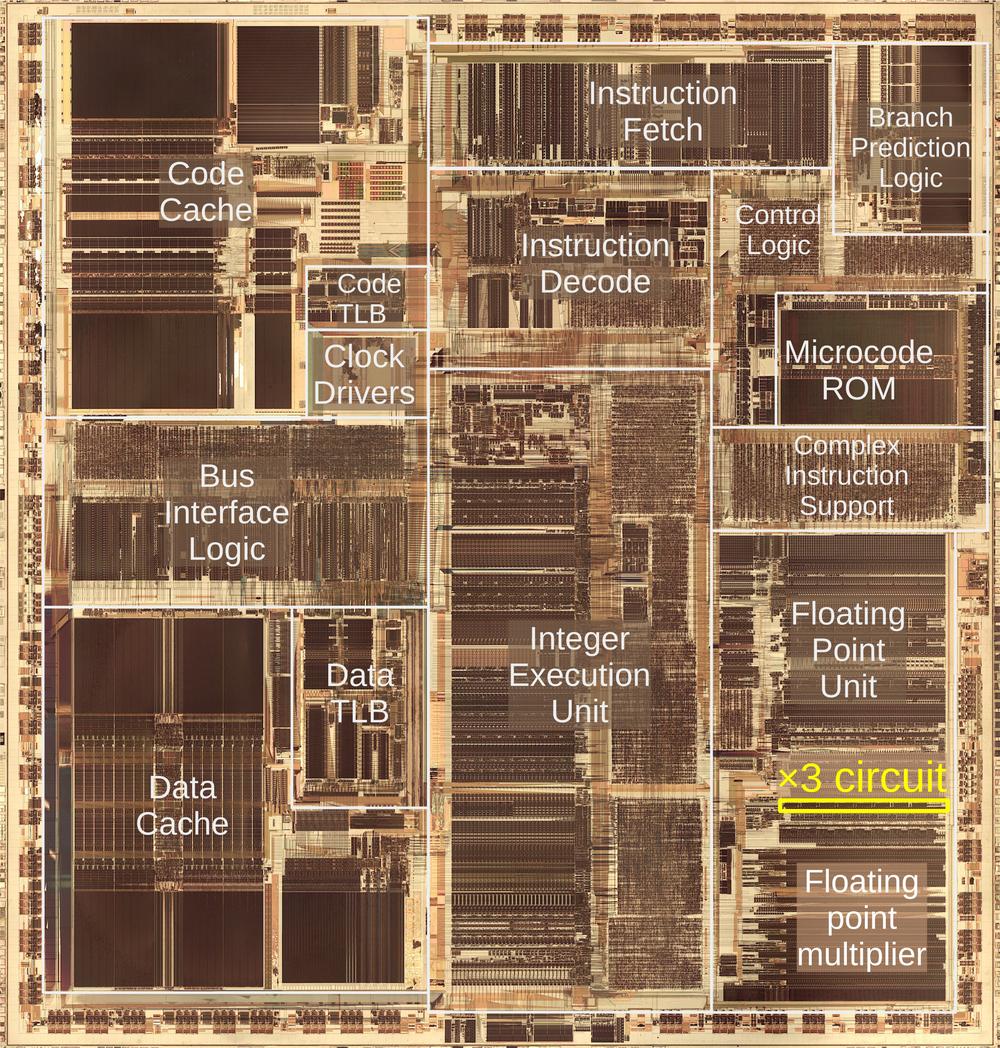
The photo below shows the Pentium's thumbnail-sized silicon die under a microscope. I've labeled the main functional blocks. In the center is the integer execution unit that performs most instructions. On the left, the code and data caches improve memory performance. The floating point unit, in the lower right, performs floating point operations. Almost half of the floating point unit is occupied by the multiplier, which uses an array of adders to rapidly multiply two 64-bit numbers. The focus of this article is the ×3 circuit, highlighted in yellow near the top of the multiplier. As you can see, the ×3 circuit takes up a nontrivial amount of the Pentium die, especially considering that its task seems simple.
Why does the Pentium use base-8 to multiply numbers?
Multiplying two numbers in binary is conceptually straightforward. You can think of binary multiplication as similar to grade-school long multiplication, but with binary numbers instead of decimal numbers. The example below shows how 5×6 is computed in binary: the three terms are added to produce the result. Conveniently, each term is either the multiplicand (101 in this case) or 0, shifted appropriately, so computing the terms is easy.
     101
    ×110
     ―――
     000    i.e. 0×101
    101     i.e. 1×101
  +101      i.e. 1×101
   ―――――
   11110
Unfortunately, this straightforward multiplication approach is slow. With the three-bit numbers above, there are three terms to add. But if you multiply two 64-bit numbers, you have 64 terms to add, requiring a lot of time and/or circuitry.
The Pentium uses a more complicated approach, computing multiplication in base 8. The idea is to consider the multiplier in groups of three bits, so instead of multiplying by 0 or 1 in each step, you multiply by a number from 0 to 7. Each term that gets added is still in binary, but the number of terms is reduced by a factor of three. Thus, instead of adding 64 terms, you add 22 terms, providing a substantial reduction in the circuitry required. (I'll describe the full details of the Pentium multiplier in a future article.2)
The downside to radix-8 multiplication is that multiplying by a number from 0 to 7 is much more complicated than multiplying by 0 or 1, which is almost trivial. Fortunately, there are some shortcuts. Note that multiplying by 2 is the same as shifting the number to the left by 1 bit position, which is very easy in hardware—you wire each bit one position to the left. Similarly, to multiply by 4, shift the multiplicand two bit positions to the left.
Multiplying by 7 seems inconvenient, but there is a trick, known as Booth's multiplication algorithm. Instead of multiplying by 7, you add 8 times the number and subtract the number, ending up with 7 times the number. You might think this requires two steps, but the trick is to multiply by one more in the (base-8) digit to the left, so you get the factor of 8 without an additional step. (A base-10 analogy is that if you want to multiply by 19, you can multiply by 20 and subtract the multiplicand.) Thus, you can get the ×7 by subtracting. Similarly, for a ×6 term, you can subtract a ×2 multiple and add ×8 in the next digit. Thus, the only difficult multiple is ×3. (What about ×5? If you can compute ×3, you can subtract that from ×8 to get ×5.)
To summarize, the Pentium's radix-8 Booth's algorithm is a fast way to multiply, but it requires a special circuit to produce the ×3 multiple of the multiplicand.
Implementing a fast ×3 circuit with carry lookahead
Multiplying a number by three is straightforward in binary: add the number to itself, shifted to the left one position. (As mentioned above, shifting to the left is the same as multiplying by two and is easy in hardware.) Unfortunately, using a simple adder is too slow.
The problem with addition is that carries make addition slow. Consider calculating 99999+1 by hand. You'll start with 9+1=10, then carry the one, generating another carry, which generates another carry, and so forth, until you go through all the digits. Computer addition has the same problem: If you're adding two numbers, the low-order bits can generate a carry that then propagates through all the bits. An adder that works this way—known as a ripple carry adder—will be slow because the carry has to ripple through all the bits. As a result, CPUs use special circuits to make addition faster.
One solution is the carry-lookahead adder. In this adder, all the carry bits are computed in parallel, before computing the sums. Then, the sum bits can be computed in parallel, using the carry bits. As a result, the addition can be completed quickly, without waiting for the carries to ripple through the entire sum.
It may seem impossible to compute the carries without computing the sum first, but there's a way to do it.
For each bit position, you determine signals called "carry generate" and "carry propagate".
These signals can then be used to determine all the carries in parallel.
The generate signal indicates that the position generates a carry. For instance, if you add binary
1xx and 1xx (where x is an arbitrary bit), a carry will be generated from the top bit,
regardless of the unspecified bits.
On the other hand, adding 0xx and 0xx will never generate a carry.
Thus, the generate signal is produced for the first case but not the second.
But what about 1xx plus 0xx? We might get a carry, for instance, 111+001, but we might not,
for instance, 101+001. In this "maybe" case, we set the carry propagate signal, indicating that a carry into the
position will get propagated out of the position. For example, if there is a carry out of
the middle position, 1xx+0xx will have a carry from the top bit. But if there is no carry out of the middle position, then
there will not be a carry from the top bit. In other words, the propagate signal indicates that a carry into the top bit will be propagated out of the top
bit.
To summarize, adding 1+1 will generate a carry. Adding 0+1 or 1+0 will propagate a
carry.
Thus, the generate signal is formed at each position by Gn = An·Bn, where A and B are the inputs.
The propagate signal is Pn = An+Bn,
the logical-OR of the inputs.3
Now that the propagate and generate signals are defined, some moderately complex logic4 can compute the carry Cn into each bit position. The important thing is that all the carry bits can be computed in parallel, without waiting for the carry to ripple through each bit position. Once each carry is computed, the sum bits can be computed in parallel: Sn = An ⊕ Bn ⊕ Cn. In other words, the two input bits and the computed carry are combined with exclusive-or. Thus, the entire sum can be computed in parallel by using carry lookahead. However, there are complications.
Implementing carry lookahead with a parallel prefix adder
The carry bits can be generated directly from the G and P signals. However, the straightforward approach requires too much hardware as the number of bits increases. Moreover, this approach needs gates with many inputs, which are slow for electrical reasons. For these reasons, the Pentium uses two techniques to keep the hardware requirements for carry lookahead tractable. First, it uses a "parallel prefix adder" algorithm for carry lookahead across 8-bit chunks.7 Second, it uses a two-level hierarchical approach for carry lookahead: the upper carry-lookahead circuit handles eight 8-bit chunks, using the same 8-bit algorithm.5
The photo below shows the complete ×3 circuit; you can see that the circuitry is divided into blocks of 8 bits. (Although I'm calling this a 64-bit circuit, it really produces a 69-bit output: there are 5 "extra" bits on the left to avoid overflow and to provide additional bits for rounding.)
The idea of the parallel-prefix adder is to
produce the propagate and generate signals across ranges of bits, not just single bits as before.
For instance, the propagate signal P32 indicates that a carry in to bit 2 would be propagated out of bit 3,
(This would happen with 10xx+01xx, for example.)
And G30 indicates that bits 3 to 0 generate a carry out of bit 3.
(This would happen with 1011+0111, for example.)
Using some mathematical tricks,6 you can take the P and G values for two smaller ranges and merge them into the P and G values for the combined range. For instance, you can start with the P and G values for bits 0 and 1, and produce P10 and G10, the propagate and generate signals describing two bits. These could be merged with P32 and G32 to produce P30 and G30, indicating if a carry is propagated across bits 3-0 or generated by bits 3-0. Note that Gn0 tells us if a carry is generated into bit n+1 from all the lower bits, which is the Cn+1 carry value that we need to compute the final sum. This merging process is more efficient than the "brute force" implementation of the carry-lookahead logic since logic subexpressions can be reused.
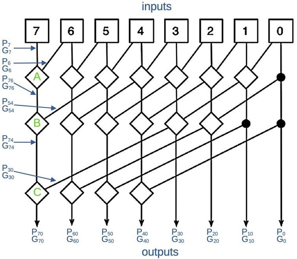
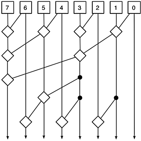
There are many different ways that you can combine the P and G terms to generate the necessary terms.8 The Pentium uses an approach called Kogge-Stone that attempts to minimize the total delay while keeping the amount of circuitry reasonable. The diagram below is the standard diagram that illustrates how a Kogge-Stone adder works. It's rather abstract, but I'll try to explain it. The diagram shows how the P and G signals are merged to produce each output at the bottom. Each square box at the top generates the P and G signals for that bit. Each line corresponds to both the P and the G signal. Each diamond combines two ranges of P and G signals to generate new P and G signals for the combined range. Thus, the signals cover wider ranges of bits as they progress downward, ending with the Gn0 outputs that indicate carries.
I've labeled a few of the intermediate signals so you can get an idea of how it works. Circuit "A" combines P7 and G7 with P6 and G6 to produce the signals describing two bits: P76 and G76. Similarly, circuit "B" combines P76 and G76 with P54 and G54 to produce the signals describing four bits: P74 and G74. Finally, circuit "C" produces the final outputs for bit 7: P70 and G70. Note that most of the intermediate results are used twice, reducing the amount of circuitry. Moreover, there are at most three levels of combination circuitry, reducing the delay compared to a deeper network.
The key point is the P and G values are computed in parallel so the carry bits can all be computed in parallel, without waiting for the carry to ripple through all the bits. (If this explanation doesn't make sense, see my discussion of the Kogge-Stone adder in the Pentium's division circuit for a different—but maybe still confusing—explanation.)
Recursive Kogge-Stone lookahead
The Kogge-Stone approach can be extended to 64 bits, but the amount of circuitry and wiring becomes overwhelming. Instead, the Pentium uses a recursive, hierarchical approach with two levels of Kogge-Stone lookahead. The lower layer uses eight Kogge-Stone adders as described above, supporting 64 bits in total.
The upper layer uses a single eight-bit Kogge-Stone lookahead circuit, treating each of the lower chunks as a single bit. That is, a lower chunk has a propagate signal P indicating that a carry into the chunk will be propagated out, as well as a generate signal G indicating that the chunk generates a carry. The upper Kogge-Stone circuit combines these chunked signals to determine if carries will be generated or propagated by groups of chunks.9
To summarize, each of the eight lower lookahead circuits computes the carries within an 8-bit chunk. The upper lookahead circuit computes the carries into and out of each 8-bit chunk. In combination, the circuits rapidly provide all the carries needed to compute the 64-bit sum.
The carry-select adder
Suppose you're on a game show: "What is 553 + 246 + c? In 10 seconds, I'll tell you if c is 0 or 1 and whoever gives the answer first wins $1000." Obviously, you shouldn't just sit around until you get c. You should do the two sums now, so you can hit the buzzer as soon as c is announced. This is the concept behind the carry-select adder: perform two additions—with a carry-in and without--and then supply the correct answer as soon as the carry is available. The carry-select adder requires additional hardware—two adders along with a multiplexer to select the result—but it overlaps the time to compute the sum with the time to compute the carry. In effect, the addition and the carry lookahead operations are performed in parallel, with the multiplexer combining the results from each.
The Pentium uses a carry-select adder for each 8-bit chunk in the ×3 circuit. The carry from the second-level carry-lookahead selects which sum should be produced for the chunk. Thus, the time to compute the carry is overlapped with the time to compute the sum.
Putting the adder pieces together
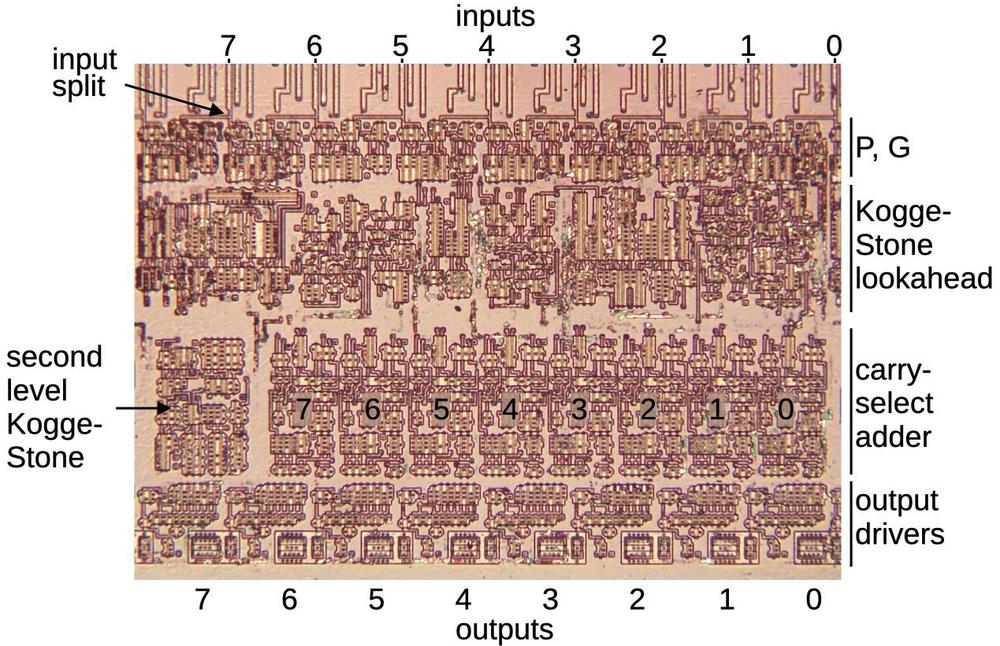
The image below zooms in on an 8-bit chunk of the ×3 multiplier, implementing an 8-bit adder. Eight input lines are at the top (along with some unrelated wires). Note that each input line splits with a signal going to the adder on the left and a signal going to the right. This is what causes the adder to multiply by 3: it adds the input and the input shifted one bit to the left, i.e. multiplied by two. The top part of the adder has eight circuits to produce the propagate and generate signals. These signals go into the 8-bit Kogge-Stone lookahead circuit. Although most of the adder consists of a circuit block repeated eight times, the Kogge-Stone circuitry appears chaotic. This is because each bit of the Kogge-Stone circuit is different—higher bits are more complicated to compute than lower bits.
The lower half of the circuit block contains an 8-bit carry-select adder. This circuit produces two sums, with multiplexers selecting the correct sum based on the carry into the block. Note that the carry-select adder blocks are narrower than the other circuitry.10 This makes room for a Kogge-Stone block on the left. The second level Kogge-Stone circuitry is split up; the 8-bit carry-lookahead circuitry has one bit implemented in each block of the adder, and produces the carry-in signal for that adder block. In other words, the image above includes 1/8 of the second-level Kogge-Stone circuit. Finally, eight driver circuits amplify the output bits before they are sent to the rest of the floating-point multiplier.
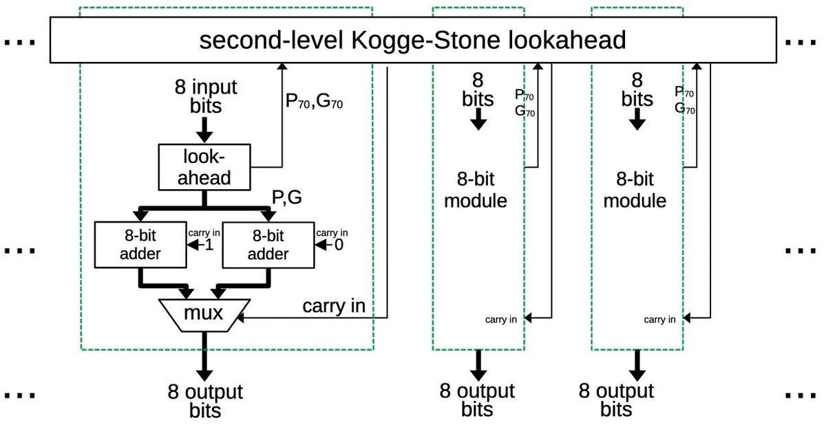
The block diagram below shows the pieces are combined to form the ×3 multiplier. The multiplier has eight 8-bit adder blocks (green boxes, corresponding to the image above). Each block computes eight bits of the total sum. Each block provides P70 and G70 signals to the second-level lookahead, which determines if each block receives a carry in. The key point to this architecture is that everything is computed in parallel, making the addition fast.
In the diagram above, the first 8-bit block is expanded to show its contents. The 8-bit lookahead circuit generates the P and G signals that determine the internal carry signals. The carry-select adder contains two 8-bit adders that use the carry lookahead values. As described earlier, one adder assumes that the block's carry-in is 1 and the second assumes the carry-in is 0. When the real carry in value is provided by the second-level lookahead circuit, the multiplexer selects the correct sum.
The photo below shows how the complete multiplier is constructed from 8-bit blocks. The multiplier produces a 69-bit output; there are 5 "extra" bits on the left. Note that the second-level Kogge-Stone blocks are larger on the right than the left since the lookahead circuitry is more complex for higher-order bits.
Going back to the full ×3 circuit above, you can see that the 8 bits on the right have significantly simpler circuitry. Because there is no carry-in to this block, the carry-select circuitry can be omitted. The block's internal carries, generated by the Kogge-Stone lookahead circuitry, are added using exclusive-NOR gates. The diagram below shows the implementation of an XNOR gate, using inverters and a multiplexer.
The XNOR circuit
I'll now describe one of the multiplier's circuits at the transistor level, in particular an XNOR gate. It's interesting to look at XNOR because XNOR (like XOR) is a tricky gate to implement and different processors use very different approaches. For instance, the Intel 386 implements XOR from AND-NOR gates (details) while the Z-80 uses pass transistors (details). The Pentium, on the other hand, uses a multiplexer.
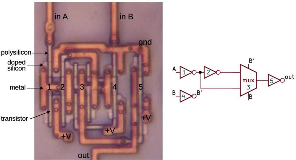
The diagram above shows one of the XNOR gates in the adder's low bits.11 The gate is constructed from four inverters and a pass-transistor multiplexer. Input B selects one of the multiplexer's two inputs: input A or input A inverted. The result is the XNOR function. (Inverter 1 buffers the input, inverter 5 buffers the output, and inverter 4 provides the complemented B signal to drive the multiplexer.)
For the photo, I removed the top two metal layers from the chip, leaving the bottom metal layer, called M1. The doped silicon regions are barely visible beneath the metal. When a polysilicon line crosses doped silicon, it forms the gate of a transistor. This CMOS circuit has NMOS transistors at the top and PMOS transistors at the bottom. Each inverter consists of two transistors, while the multiplexer consists of four transistors.
The BiCMOS output drivers
The outputs from the ×3 circuit require high current. In particular, each signal from the ×3 circuit can drive up to 22 terms in the floating-point multiplier. Moreover, the destination circuits can be a significant distance from the ×3 circuit due to the size of the multiplier. Since the ×3 signals are connected to many transistor gates through long wires, the capacitance is high, requiring high current to change the signals quickly.
The Pentium is constructed with a somewhat unusual process called BiCMOS, which combines bipolar transistors and CMOS on the same chip. The Pentium extensively uses BiCMOS circuits since they reduced signal delays by up to 35%. Intel also used BiCMOS for the Pentium Pro, Pentium II, Pentium III, and Xeon processors. However, as chip voltages dropped, the benefit from bipolar transistors dropped too and BiCMOS was eventually abandoned.
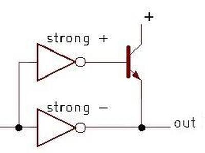
The schematic below shows a simplified BiCMOS driver that inverts its input. A 0 input turns on the upper inverter, providing current into the bipolar (NPN) transistor's base. This turns on the transistor, causing it to pull the output high strongly and rapidly. A 1 input, on the other hand, will stop the current flow through the NPN transistor's base, turning it off. At the same time, the lower inverter will pull the output low. (The NPN transistor can only pull the output high.)
Note the asymmetrical construction of the inverters. Since the upper inverter must provide a large current into the NPN transistor's base, it is designed to produce a strong (high-current) positive output and a weak low output. The lower inverter, on the other hand, is responsible for pulling the output low. Thus, it is constructed to produce a strong low output, while the high output can be weak.
The driver of the ×3 circuit goes one step further: it uses a BiCMOS driver to drive a second BiCMOS driver. The motivation is that the high-current inverters have fairly large transistor gates, so they need to be driven with high current (but not as much as they produce, so there isn't an infinite regress).12
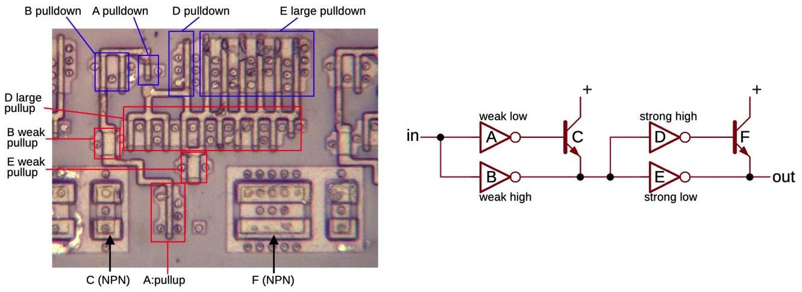
The schematic below shows the BiCMOS driver circuit that the ×3 multiplier uses. Note the large, box-like appearance of the NPN transistors, very different from the regular MOS transistors. Each box contains two NPN transistors sharing collectors: a larger transistor on the left and a smaller one on the right. You might expect these transistors to work together, but the contiguous transistors are part of two separate circuits. Instead, the small NPN transistor to the left and the large NPN transistor to the right are part of the same circuit.
The inverters are constructed as standard CMOS circuits with PMOS transistors to pull the output high and NMOS transistors to pull the output low. The inverters are carefully structured to provide asymmetrical current, making them more interesting than typical inverters. Two pullup transistors have a long gate, making these transistors unusually weak. Other parts of the inverters have multiple transistors in parallel, providing more current. Moreover, the inverters have unusual layouts, with the NMOS and PMOS transistors widely separated to make the layout more efficient. For more on BiCMOS in the Pentium, see my article on interesting BiCMOS circuits in the Pentium.
Conclusions
Hardware support for computer multiplication has a long history going back to the 1950s.13 Early microprocessors, though, had very limited capabilities, so microprocessors such as the 6502 didn't have hardware support for multiplication; users had to implement multiplication in software through shifts and adds. As hardware advanced, processors provided multiplication instructions but they were still slow. For example, the Intel 8086 processor (1978) implemented multiplication in microcode, performing a slow shift-and-add loop internally. Processors became exponentially more powerful over time, as described by Moore's Law, allowing later processors to include dedicated multiplication hardware. The 386 processor (1985) included a multiply unit, but it was still slow, taking up to 41 clock cycles for a multiplication instruction.
By the time of the Pentium (1993), microprocessors contained millions of transistors, opening up new possibilities for design. With a seemingly unlimited number of transistors, chip architects could look at complicated new approaches to squeeze more performance out of a system. This ×3 multiplier contains roughly 9000 transistors, a bit more than an entire Z80 microprocessor (1976). Keep in mind that the ×3 multiplier is a small part of the floating-point multiplier, which is part of the floating-point unit in the Pentium. Thus, this small piece of a feature is more complicated than an entire microprocessor from 17 years earlier, illustrating the incredible growth in processor complexity.
I plan to write more about the implementation of the Pentium, so follow me on Bluesky (@righto.com) or RSS for updates. (I'm no longer on Twitter.) The Pentium Navajo rug inspired me to examine the Pentium in more detail.
Footnotes and references
-
A floating-point multiplication on the Pentium takes three clock cycles, of which the multiplication circuitry is busy for two cycles. (See Agner Fog's optimization manual.) In comparison, integer multiplication (
MUL) is much slower, taking 11 cycles. The Nehalem microarchitecture (2008) reduced floating-point multiplication time to 1 cycle. ↩ -
I'll give a quick outline of the Pentium's floating-point multiplier as a preview. The multiplier is built from a tree of ten carry-save adders to sum the terms. Each carry-save adder is a 4:2 compression adder, taking four input bits and producing two output bits. The output from the carry-save adder is converted to the final result by an adder using Kogge-Stone lookahead and carry select. Multiplying two 64-bit numbers yields 128 bits, but the Pentium produces a 64-bit result. (There are actually a few more bits for rounding.) The low 64 bits can't simply be discarded because they could produce a carry into the preserved bits. Thus, the low 64 bits go into another Kogge-Stone lookahead circuit that doesn't produce a sum, but indicates if there is a carry. Since the datapath is 64 bits wide, but the product is 128 bits, there are many shift stages to move the bits to the right column. Moreover, the adders are somewhat wider than 64 bits as needed to hold the intermediate sums. ↩
-
The bits
1+1will set generate, but should propagate be set too? It doesn't make a difference as far as the equations. This adder sets propagate for1+1but some other adders do not. The answer depends on if you use an inclusive-or or exclusive-or gate to produce the propagate signal. ↩ -
The carry Cn at each bit position n can be computed from the G and P signals by considering the various cases:
C1 = G0: a carry into bit 1 occurs if a carry is generated from bit 0.
C2 = G1 + G0P1: A carry into bit 2 occurs if bit 1 generates a carry or bit 1 propagates a carry from bit 0.
C3 = G2 + G1P2 + G0P1P2: A carry into bit 3 occurs if bit 2 generates a carry, or bit 2 propagates a carry generated from bit 1, or bits 2 and 1 propagate a carry generated from bit 0.
C4 = G3 + G2P3 + G1P2P3 + G0P1P2P3: A carry into bit 4 occurs if a carry is generated from bit 3, 2, 1, or 0 along with the necessary propagate signals.
And so on...Note that the formula gets more complicated for each bit position. The circuit complexity is approximately O(N3), depending on how you measure it. Thus, implementing the carry lookahead formula directly becomes impractical as the number of bits gets large. The Kogge-Stone approach uses approximately O(N log N) transistors, but the wiring becomes excessive for large N since there are N/2 wires of length N/2. Using a tree of Kogge-Stone circuits reduces the amount of wiring. ↩
-
The 8-bit chunks in the circuitry have nothing to do with bytes. The motivation is that 8 bits is a reasonable size for a chunk, as well as providing a nice breakdown into 8 chunks of 8 bits. Other systems have used 4-bit chunks for carry lookahead (such as minicomputers based on the 74181 ALU chip). ↩
-
I won't go into the mathematics of merging P and G signals; see, for example, Adder Circuits or Carry Lookahead Adders for additional details. The important factor is that the carry merge operator is associative (actually a monoid), so the sub-ranges can be merged in any order. This flexibility is what allows different algorithms with different tradeoffs. ↩
-
The idea behind a prefix adder is that we want to see if there is a carry out of bit 0, bits 0-1, bits 0-2, bits 0-3, 0-4, and so forth. These are all the prefixes of the word. Since the prefixes are computed in parallel, it's called a parallel prefix adder. ↩
-
The lookahead merging process can be implemented in many ways, including Kogge-Stone, Brent-Kung, and Ladner-Fischer, with different tradeoffs. For one example, the diagram below shows that Brent-Kung uses fewer "diamonds" but more layers. Thus, a Brent-Kung adder uses less circuitry but is slower. (You can follow each output upward to verify that the tree reaches the correct inputs.)
A diagram of an 8-bit Brent-Kung adder. Diagram by Robey Pointer, Wikimedia Commons. -
The higher-level Kogge-Stone lookahead circuit uses the eight P70 and G70 signals from the eight lower-level lookahead circuits. Note that P70 and G70 indicate that an 8-bit chunk will propagate or generate a carry. The higher-level lookahead circuit treats 8-bit chunks as a unit, while the lower-level lookahead circuit treats 1-bit chunks as a unit. Thus, the higher-level and lower-level lookahead circuits are essentially identical, acting on 8-bit values. ↩
-
The floating-point unit is built from fixed-width columns, one for each bit. Each column is 38.5 µm wide, so the circuitry in each column must be designed to fit that width. For the most part, the same circuitry is repeated for each of the 64 (or so) bits. The carry-select adder is unusual since it doesn't follow the column width of the rest of the floating-point unit. Instead, it crams 8 circuits into the width of 6.5 regular circuits. This leaves room for one Kogge-Stone circuitry block. ↩
-
Because there is no carry-in to the lowest 8-bit block of the ×3 circuit, the carry-select circuit is not needed. Instead, each output bit can be computed using an XNOR gate. ↩
-
The principle of Logical Effort explains that for best performance, you don't want to jump from a small signal to a high-current signal in one step. Instead, a small signal produces a medium signal, which produces a larger signal. By using multiple stages of circuitry, the overall delay can be reduced. ↩
-
The Booth multiplication technique was described in 1951, while parallel multipliers were proposed in the mid-1960s by Wallace and Dadda. Jumping ahead to higher-radix multiplication, a 1992 paper A Fast Hybrid Multiplier Combining Booth and Wallace/Dadda Algorithms from Motorola discusses radix-4 and radix-8 algorithms for a 32-bit multiplier, but decides that computing the ×3 multiple makes radix-8 impractical. IBM discussed a 32-bit multiplier in 1997: A Radix-8 CMOS S/390 Multiplier. Bewick's 1994 PhD thesis Fast Multiplication: Algorithms and Implementation describes numerous algorithms.
For adders, Two-Operand Addition is an interesting presentation on different approaches. CMOS VLSI Design has a good discussion of addition and various lookahead networks. It summarizes the tradeoffs: "Brent-Kung has too many logic levels. Sklansky has too much fanout. And Kogge-Stone has too many wires. Between these three extremes, the Han-Carlson, Ladner-Fischer, and Knowles trees fill out the design space with different compromises between number of stages, fanout, and wire count." The approach used in the Pentium's ×3 multiplier is sometimes called a sparse-tree adder. ↩

17 comments:
So detailed and learnt so many things. I wish there would be any newsletter to read all your blogs?
If yes can you include my email [email protected]?
I want to thank you for this. The First CPU I purchased was the Pentium 75hz, Which I overclocked to 83z. It was the fist PC I built, when I was in highschool. This was so detailed & informative, niche, & dense I had to read it 3 times. But I love it. Thanks again.
Thank you very much for this in-depth post. It is incredible, though I want to know, did you get the whole information of the technology by just reverse engineering the die under microscope? It's really amazing.
Advancing bytes into code via switches to an 8080 was my early 80s introduction to coding. Reducing code cycles to sample audio on a cm64 6052 next. Then an Atari with an assembler Wow. Now copilot knows what I'm trying to do in pretty much any language. But I love this article cos I came from the electronics side into computing.
I forced my pentium 90 to do 125Mhz nearly all of its life. Its amazing how all this ingenuity is baked in there, and I wonder if on new designs these solutions are baked in to the generation of the design or if we've got to the stage where we favour complexity. I say this because new designs are so complex that we have to rely on it being mostly generated rather than had crafted. But I don't really know as I stopped following advances in the early 2000s.
I can see that base-8 multiplying makes sense but I would have thought that an easy way to do this would be a look-up table of all the results - there are only 64 of them after all. Why did they go to all this trouble of bit shifting and adding when a single memory lookup using a rather small table would solve the problem?
"Why did they go to all this trouble of bit shifting and adding when a single memory lookup using a rather small table would solve the problem?"
I would assume that they didn't do that because it wouldn't actually solve the problem. Using a lookup table for all of the 3 bit by 3 bit multiplications, giving a 6 bit result would have to be duplicated 22 times (otherwise, you'd have to wait for each 3 bit piece to complete before processing the next 3 bit piece). And you'd still have the 22 intermediate results needing to be added together to finish the multiplication. What the multiplication is doing is repeating the following 22 times
add multiplicand multiplied by by next 3 bits of multiplier to sum
shift sum and multiplier by 3 bits
What your idea does is replace the first step with something that's actually more complicated and slower.
I don't know. I doubt there is any 3 bits multiplier in Pentium. From where did you get that info? In picture of multiplier (long purple picture) there are 8 serial peaces and each of those 8 peaces have 8 bits. So total 8*8 = 64 bits. I think for Pentium time procesor, there could be 8 lines of 64 bits where each line shifted by 1 to right more (first line shifted by 7 bits positions to right, second line shifted by 6 bits positions to right, third - by 5 positions, 4th - by 4, 5th - by 3, 6th - by 2, 7th - by 1, 8th - not shifted; up to 7 bits shifted out don't make almost any difference to final result). When Floating point unit doing multiplication, then it passes 64 bits to 8 64 bits lines and then adds those line (where each line shifted in circuit by some number from 0 to 7). Then in one cycle it makes add operation of all lines. Then bits in all lines shifted to right by one position and then binary values in 8 lines added toghether. This result added to previous result of 8 64 bit lines add operation. Then again everything shifted to left by 1 position and again all lines added. So total need to shift 8 times and to add 8+8=16 times total. This would produce multiplication of 64 bits by 64 bits. Shifted out bits very weakly impact on final result and precision loss in worst case will be few last bits. And calulating carry signals through propogation from bit to bit doesn't looks too complex, but maybe your mentioned methods good too or better.
Then again everything shifted to RIGHT by 1 position and again all lines added.
Also From each of 8 peaces of 8 bits need to see what bits are in 8bits one peace. This 8 bits controling 8 lines and depening of each of 8 bits value (0 or 1), the lines have either first operand (of 64 bits) if corresponding bit is 1 or all zeros if corrsponding bit is 0 from one peace. And during all shifting and adding need to propagate each time one of 8 peaces of second operand, which controls what will it be in line - the first operand or zeros. Second operand is controling operand, but here additional complexity ocurs, because need to switch on second operand (of 64 bits) to some peace (of 8 bits) for controling the lines (with zeros or with first operand)... So better just made normal 64 lines of 64 bits, where each higher line shifted one bit possition more to right. Then add gates adding all bits of two lines and making carry and somehow need to insert small capacitor so carry go all the way to the left and addition to third line would be delayed (because of this capacitor scheme)... Because CPU don't have problems to add two binary numbers and propagate carry from bit to bit to most left bit - to carry bit. There actualy 8087 could do such addition of all line in one cycle, which is multiplication of two 64 bits numbers. But maybe all latency comes from 16 bits data bus, through which loaded 64 bits numbers to 8087. And from exponent operations...
If x7 is implemented as x8-1, why x3 isn't done as x4-1 instead of all this complicated stuff ?
by32768: The trick is that the ×8 term isn't explicitly added; the Booth's algorithm just multiplies by one more in the next digit, which gives you ×8 because you're using radix-8. To do ×4-1 would require putting ×4 and -1× into an adder, so you'd need another adder for each stage.
Anonymous: I reverse-engineered the circuitry of the adder by studying the chip under a microscope to determine how it works, so there's no need for you to make up alternative explanations.
Something definetly wrong about like you write in begining "Thus, instead of adding 64 terms, you add 22 terms, providing a substantial reduction in the circuitry required."
This would mean that Pentium calculating not in binary and not in decimal system, and not in hexodecimal (from 0 to 15), but in octadecimal system (from 0 to 7). And this means 3 bits is one number. Is that right? 3*22=66 bits of precision.
I think more realistic is that if this x3 multiplier exist, then all his purpose is to multiply whole number only by 3. Can't multiply by 9 (unless can decode it as twice x3) or by 23 or by 30. Number 3 in binary is ...00011. So in begining there are just two lines and one of them shifted one possition to left or right and all over lines don't needed because everywhere in number "...000011" is zeros in begining. Then Those two 64 bits lines (or 69 bits etc) added together (one of them shifted to some side predefined in circuit). This is multiplication by 3 with binary numbers. If need multiply by 8 then also possible to shift 64 bits of mantisa by 3 places to left. In need multiply by 256 (2^8=256) then need to shift all 64 mantisa bits to left by 8 bits or one byte. To multiply by big number like 5425481325, then normal 64 bits with 64 lines multiplier (where each line shifted to left more than precious and then all lines added...) needed. So you tricks like multiply by 7 is like multiply by 8 (whichs is 3 times shift to left) and then subtract 64 bits number could be dedicated only for fast multiplication by SMALL numbers (from 2 to 7, I pressume) .
Maybe now I get it. You saying there is 22 lines which do that? And each this line shifted by 3 bits to left more than previous line? Then at the end all this 22 lines added? So then each line like multiply by "from 0 to 7 number" line kinda operator? Doesn't it makes multiplication circuit even more complex? OR each of 22 lines handled separatly and need at least 22 two cycles for multiplication (of two 64 bits numbers)?
Surely multiplying by 3 can be done faster than adding 2x and x using a general-purpose adder circuit? For example, the condition for carry propagation across an 8-bit chunk with value y is just "is y equal to 0x55", and the carry generation condition from that chunk is just "is y greater than 0x55", both of which can be implemented in considerably fewer gates than an 8-bit Kogge-Stone lookahead array.
Perhaps the Intel engineers already had a 64-bit adder laid out and wanted to reuse that rather than designing something new? It would be interesting to know if the same adder layout is also used elsewhere on that die.
I don't understand this analysis. The carry generation and propagation of adding two 8-bit numbers, x and y, depends on more than just the value of y. For example, if x = 0 then no carry is generated even if y > 0x55.
Ken, excellent article, as always. Could you give an example of x7? This sentence is hard to parse "You might think this requires two steps, but the trick is to multiply by one more in the digit to the left, so you get the factor of 8 without an additional step." I"m not sure what is meant by "the digit to the left".
Hi John! I plan to write about the full multiplication algorithm soon. By "the digit to the left", I mean the base-8 group of three bits to the left of the current group of three bits. For example, suppose you're multiplying by 001111. In base-8, this is 17. Instead of multiplying by 7, you multiply by -1 and bump the next digit to 2. Multiplying by 2*8 and -1 is the same as multiplying by 8 and 7, and the result is multiplying by 15, which is what you want for 001111. Hopefully this makes sense. (An important thing is that bumping up the multipliers can be done in parallel, unlike ripple carry, so it doesn't slow things down.)
The strategy for the design of adders and multipliers depends implicitly on the relative speeds of various building blocks, such as gates, muxes, and wires.
In relay logic, for example, switching is slow, but propagation through muxes - and through wires - takes no time at all at that scale. Thus we get Zuse's adder, which has a carry ripple that is instant.
In CMOS, wires are slow and take more effort to drive the longer they are. The relative speed of propagation through a passive MUX versus switching said MUX depends on the process and mux resistance. In CD4000 family, for example, at 12V supply, muxes built out of SPST switches (4066) outperform everything else in terms of propagation time.
It may be obvious in hindsight, but an "optimal" design for a x3 adder in a Pentium will not be the same as that of an adder built out of TTL, relays, or even integrated CMOS logic on a different process node.
Post a Comment