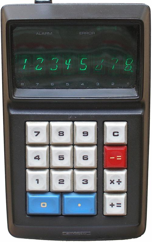
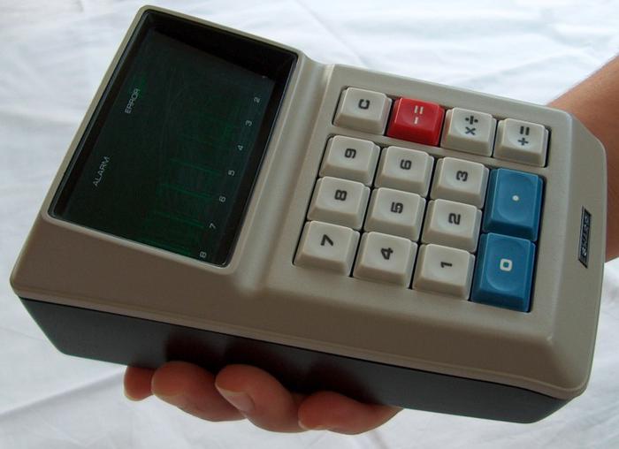
In 1969, high-density MOS integrated circuits were still new and logic circuits were constructed in a variety of ways. One technique was "four-phase logic", which provided ten times the speed and density of standard logic gates while using 1/10 the power.1 One notable application of four-phase logic was calculators. In 1969, Sharp introduced the first calculator built from high-density MOS chips, the QT-8D, followed by the world's smallest calculator, the handheld EL-8. These calculators were high-end products, selling for $345 (about $1800 today).
Integrated circuits at the time weren't dense enough to implement an entire calculator on one chip so these calculators split the functionality across five ICs. These five chips were created for Sharp by the Autonetics division of Rockwell. Autonetics invented four-phase logic in the mid-1960s, so this logic family was a natural choice for the calculator chips.
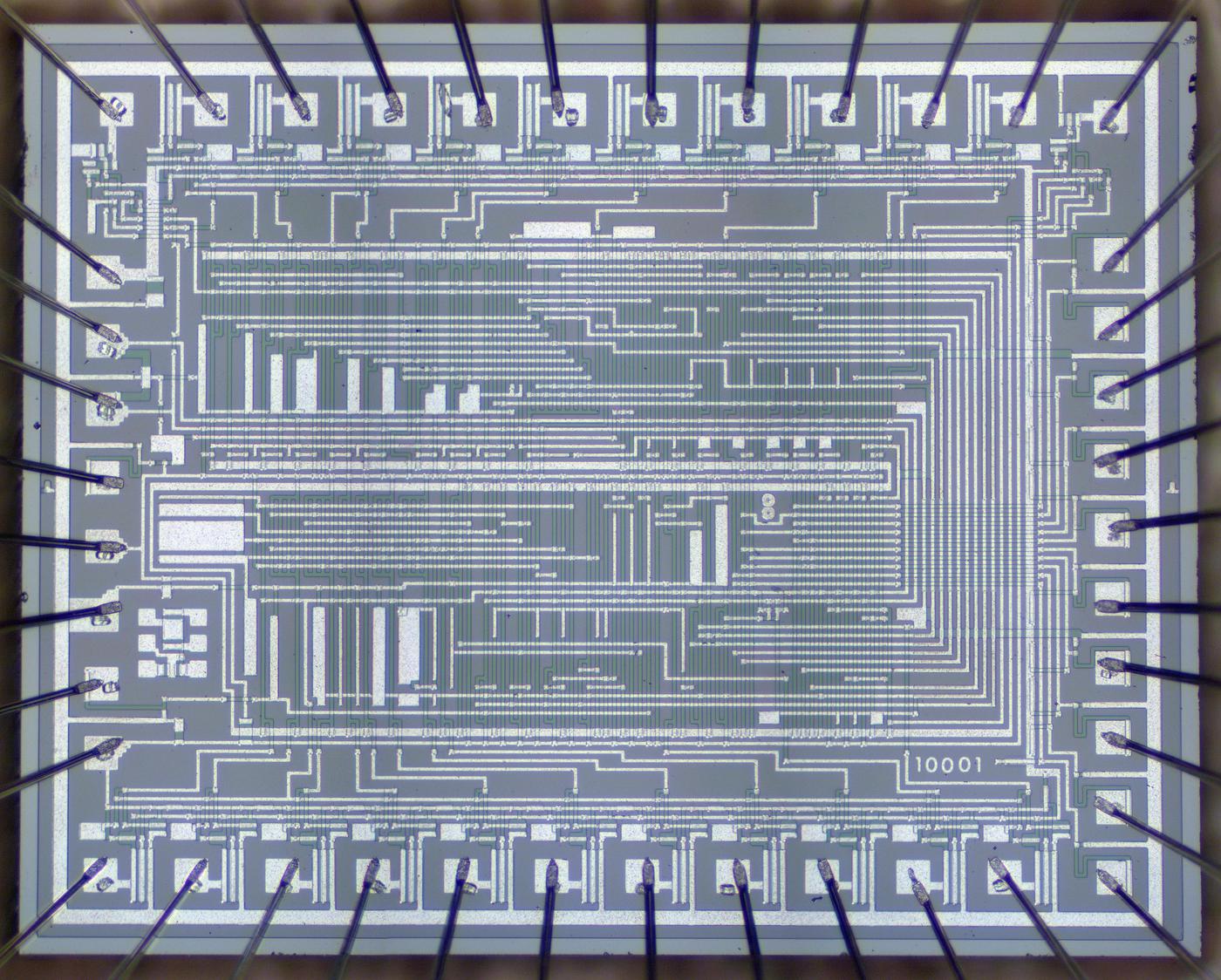
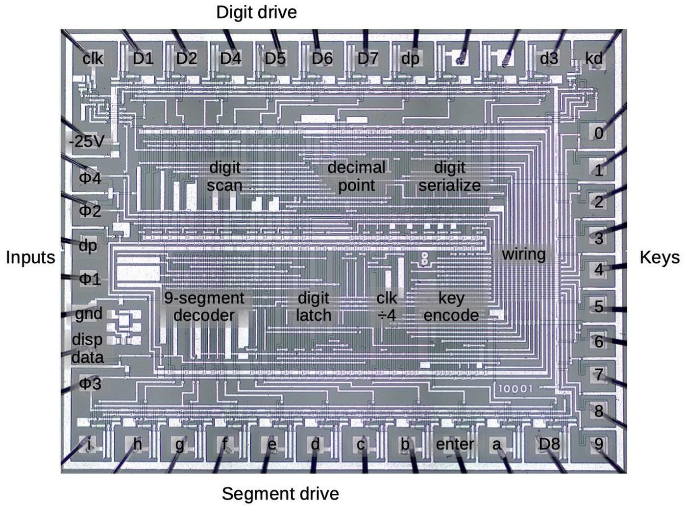
In this blog post, I reverse-engineer the keypad/display chip shown above. This photo shows the tiny silicon die under a microscope. The silicon substrate has a purple tint while the doped, conductive silicon is green. The metal layer on top is white. Around the edges, thin bond wires connect the die to the 42 external pins. The chip contains roughly 500 transistors implementing 100 logic gates. While the density of this chip is absurdly low by modern standards, it illustrates the progress of MOS integrated circuits in the late 1960s.
Inside the calculator
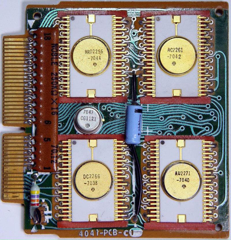
The photo below shows the circuit board inside the calculator. The board is dominated by the four large integrated circuits with circular golden lids. These integrated circuits were packaged as 42-pin ceramic ICs with staggered pins, an arrangement that provided more room for the PCB traces. Unlike modern printed circuit boards, the traces on this board are curved, showing its hand-drawn layout.
These four chips have different functions: an arithmetic chip, a decimal point chip, a keypad/display chip, and a control chip. This blog post focuses on the keypad/display chip (NRD2256) in the upper left. The fifth chip, is the clock chip in the small metal can that provides the four-phase timing pulses. The system clock runs at about 60 kilohertz, very slow by microprocessor standards, but fast enough for a calculator
One function of the keypad/display chip is to handle keypresses, converting a digit key into a 4-bit serial binary value. (Unexpectedly, non-digit keypresses are handled by other chips.) Its second main function is to display digits on the display. Like most calculators, this calculator multiplexes the display; it displays one digit at a time, repeated rapidly enough that the display appears uniform. It does this by activating one display tube at a time and energizing the appropriate segments to produce the desired digit.2
The four main chips communicate serially, sending each decimal digit as four BCD (binary-coded decimal) bits. Each communication cycle consists of 8 digits plus a ninth unused spot, forming a 36-bit "packet".3 The basic timing comes from the 60-kilohertz clock chip; one bit is sent each clock cycle. The keypad/display chip produces additional timing signals keep everything synchronized. First, it divides the clock by 4, generating a "digit clock" signal that indicates each 4-bit digit. The keypad/display chip cycles through the display digits, one digit every four clocks; it transmits signals to the other chips to keep track of the current digit. Thus, as the keypad/display chip cycles through the digits of the display, it receives the binary value of each digit at the right time.
The diagram below shows the functional units in the keypad/display chip. The "digit scan" circuitry scans through the eight digit drive lines D1-D8. The "decimal point" circuitry deserializes the decimal point input "dp" and energizes the decimal point segment when the specified digit is active. The "digit serialize" circuit converts a digit keypress into four serial bits. The "wiring" section is simply wiring between the upper half of the chip and the lower half, showing how much space is wasted by signal routing. In the lower half, the "9-segment decoder" illuminates the appropriate segments to display a digit; this digit is serialized by the "digit latch" circuit. The "clk÷4" circuit divides the input clock by four to produce the digit clock. Finally, the "key encode" circuit converts a keypress (0-9) into the four-bit value used by the "digit serialize" circuit. As will be seen, these functional blocks are not very complex, consisting of maybe 20 gates each.
PMOS Transistors
The calculator chip is built from metal-gate PMOS transistors. This type of transistor was easy to manufacture in the 1960s, but rapidly became obsolete. These transistors required large negative voltages, -25 volts for the calculator chip. (For simplicity, I will view the signals as active-low; 0V is a logical 0 and -25V is a logical 1.) Another problem with metal-gate transistors is that most of the chip was occupied by silicon and metal wiring, so the density of transistors was very low.
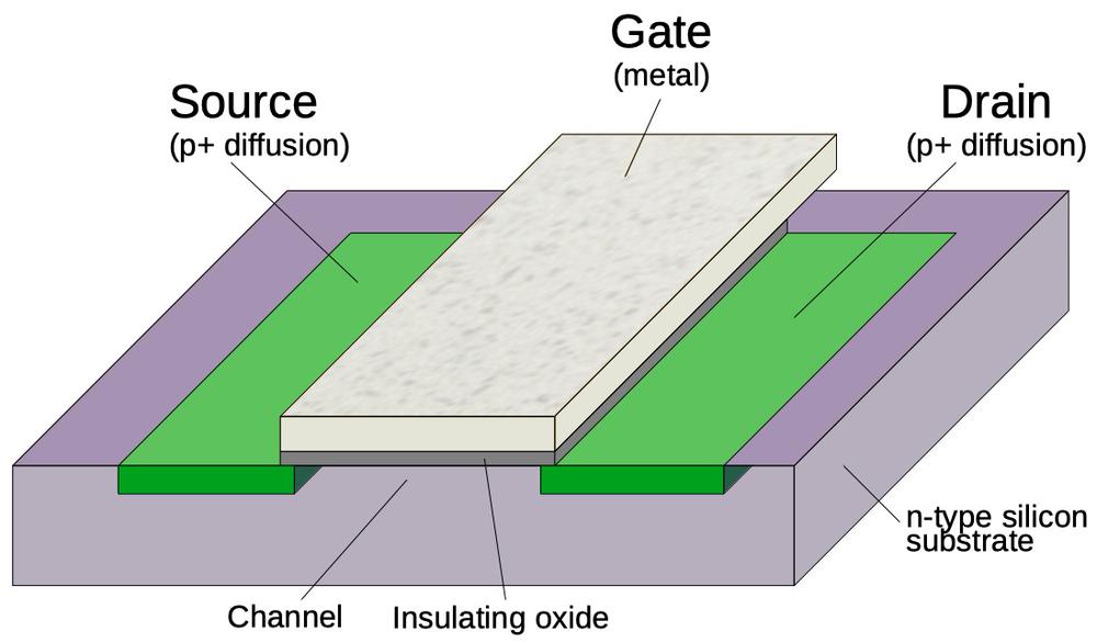
The diagram below illustrates a metal-gate PMOS transistor. At the bottom, two regions of silicon (green) are doped to make them conductive, forming the source and drain of the transistor The gate is formed by a metal strip between the silicon regions, separated from the silicon by a thin layer of insulating oxide. (These layers—Metal, Oxide, Semiconductor—give the MOS transistor its name.) The transistor can be considered a switch between the source and drain, controlled by the gate. To simplify the behavior, a PMOS transistor turns on when the gate is pulled negative (-25 volts), while the transistor turns off when the gate is at 0 volts.
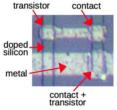
The image below shows how a transistor appears on the die. The gate is formed by the metal overlapping the doped silicon (vertical green strip). Inconveniently, a contact that connects the metal layer to the silicon looks very similar to a transistor in this chip—the metal layer in a transistor almost touches the silicon, while the metal layer in a contact touches the silicon. A contact and a transistor can be distinguished with effort; a contact is more square-shaped while a transistor is more oval-shaped and slightly blurrier. As will be explained below, four-phase logic often uses transistors where both the gate and the drain are connected to the same clock; this type of connection appears at the bottom of the diagram. By recognizing the transistors, the circuitry can be reverse-engineered.
How four-phase logic works
Four-phase logic is a technique for building logic gates, such as NAND gates. At the time, the standard way of building a logic gate was called "static logic", because the output remained constant as long as the inputs didn't change. A disadvantage of static logic was that it required a large "load transistor" that continuously used current, resulting in high power consumption.
A solution to these problems was "dynamic logic". Instead of providing a steady output from the gate, the gate's output was controlled by a clock signal. The gate's value would be computed and then stored by the circuit's capacitance, instead of requiring a continuous current. Developing with dynamic logic can be tricky, however, because of its dependence on timing. (It also has the disadvantage that the output values rapidly leak away, rather than being stable as with static logic.) Dynamic logic is still used in modern CPUs, in the form of domino logic.
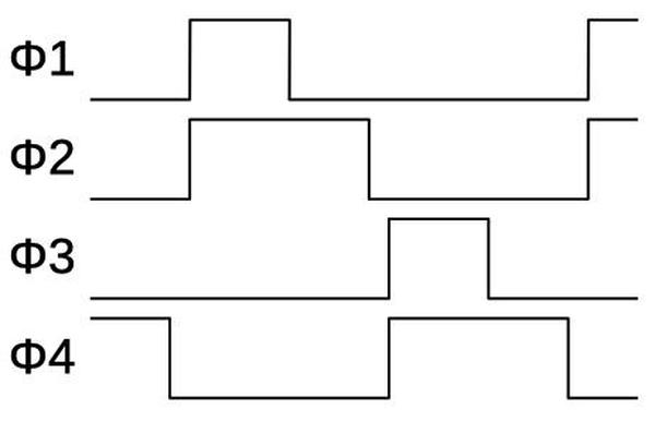
Four-phase logic is a specific type of dynamic logic, designed to simplify the design process. Its timing is controlled by four clock signals (below), the source of the name "four-phase".4 In the calculator, these clock signals repeated at 60 kilohertz.
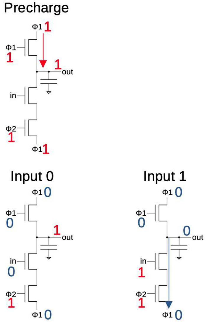
The diagram below shows how an inverter is implemented in four-phase logic. In the first clock phase, φ1 is high causing the capacitor to get charged. In the second clock phase, the gate's value is determined. If the input is 0, the capacitor keeps its previous value (1). But if the input is 1, the capacitor discharges through the lower transistors so the output is 0. Thus, the circuit inverts the input.5 The capacitor holds the output for the remainder of the clock cycle, so the gate also acts as a latch. (This is an important feature of four-phase logic, simplifying many circuits.)
More complex gates are built in a similar manner. For a NAND gate, multiple input transistors are put in series; if all inputs are 1, the capacitor will discharge and the output will be 0. For a NOR gate, multiple input transistors are put in parallel; any 1 input will yield a 0. As will be seen later, complex gates can be created with a mixture of series and parallel transistors.
The gate described above only uses two phases,6 so why four-phase logic? The problem with the above circuit is that if you connect two gates together, during step 2 the output of the first gate will be changing while the second gate is using this value. This could cause the second gate to erroneously discharge, yielding the wrong answer. The solution is for the second gate to wait until the first gate is stable. Specifically, the first gate operates during time periods 1 and 2, while the second gate operates during time periods 3 and 4. The second gate can then be safely connected to another gate operating during time periods 1 and 2. A circuit that alternates the two types of gates will operate safely.7
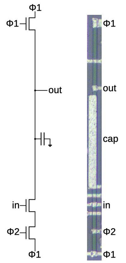
The diagram below shows how a four-phase inverter appears on the die. The schematic is the same as before, but the circuit is stretched vertically, with a layout that is tall and skinny. The inverter consists of a doped silicon line (green) running vertically, crossed by metal wiring. The gate is implemented by three small transistors. The large capacitor in the middle holds the output voltage. Dynamic logic is often built to use the stray capacitance of the wiring, but this chip uses many large capacitors (perhaps due to leakage or the slow clock speed).
Implementation of the calculator circuits
In the next sections, I'll describe how some of the calculator IC's circuits are implemented using four-phase logic.
Shift register
This chip uses shift registers to convert a serial input signal into a parallel binary value. One shift register is used for the decimal point position input while another shift register handles the digit to be displayed. The basic implementation of the shift register is a chain of inverters with two inverters per stage. Because four-phase logic is clocked, a bit will advance through the two inverters every clock cycle. (One inverter during Φ1/Φ2 and the second inverter during Φ3/Φ4.) This is an advantage of four-phase logic; standard logic requires a flip-flop at each stage to hold the bits, making the circuit much more complex. Each stage has an additional inverter to output the uncomplemented value. To keep both outputs synchronized, these inverters use special timing, precharging on Φ3 and reading on Φ1.7
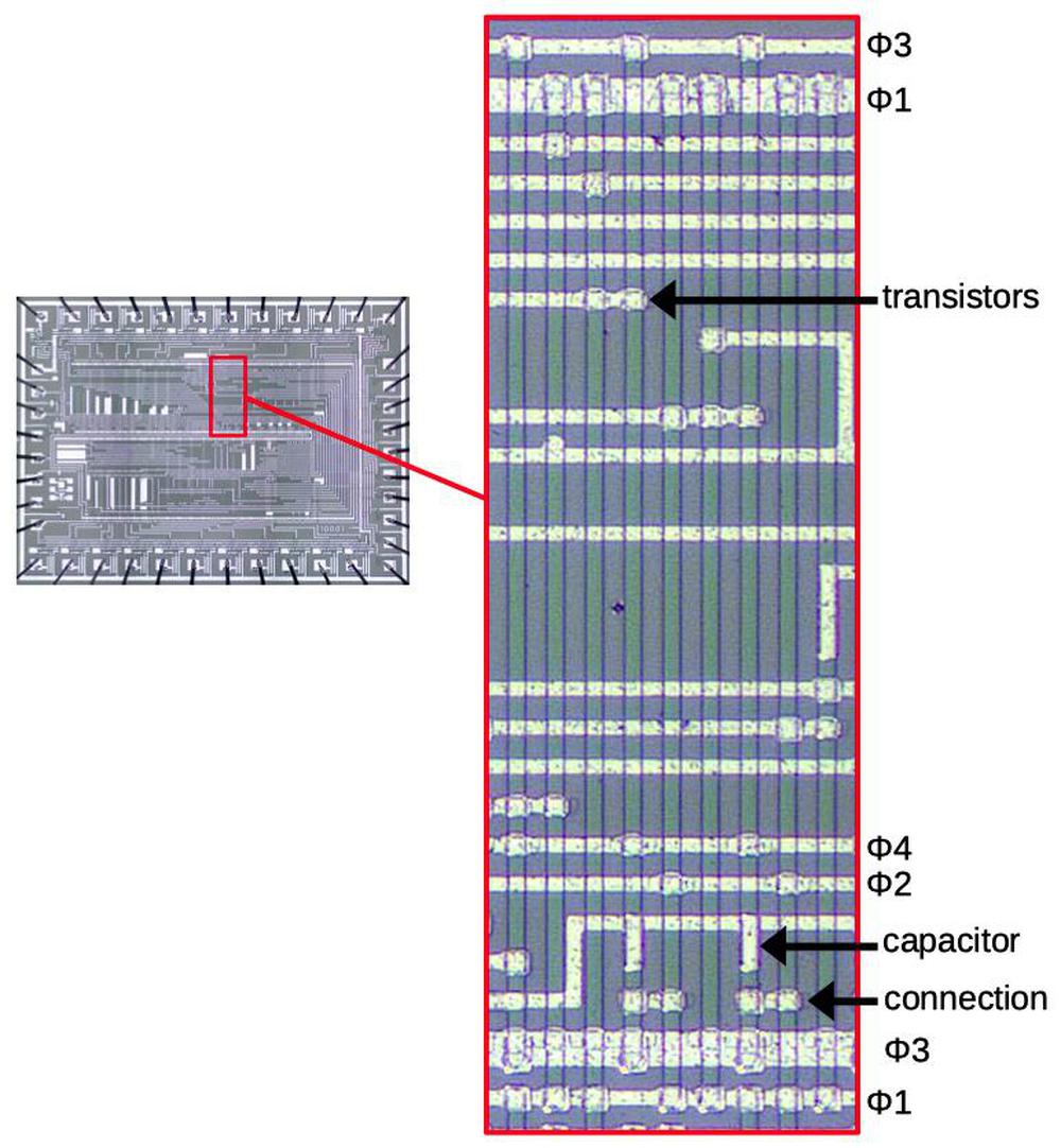
The diagram below shows how the shift register for the decimal point position is implemented on the die. It shows nine inverters, implemented with 27 transistors. Each vertical green line of doped silicon is one gate, while the white metal wiring is mostly horizontal. Note that this circuitry, just nine gates, takes up a large fraction of the die. While the gates are tightly packed side-to-side, they are very tall, so the die holds just two rows of gates. The density of transistors is very low, with most of the area consumed by wiring. Even so, four-phase logic was considered a dense way of creating gates, since other techniques were even worse. (A couple of years later, microprocessors used an additional layer of polysilicon wiring, which made signal routing much easier and greatly increased the density.)
Examples of transistors and capacitors are indicated on the diagram. At the bottom, the arrow shows one of the connections between two inverters. The short horizontal wire is connected to the inverter on the left, and forms the gate of the inverter on the right. Other wires are longer as they connect inverters to other parts of the circuitry.
Binary encoding
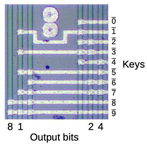
The chip converts each digit keypress into a binary encoding, using the NAND gates shown below. The calculator's buttons are magnets, closing reed switches. These switches are connected to the inputs on the right. When a key is pressed, the input goes low and the circuit generates the corresponding 4-bit binary output at the bottom.
Each vertical green line corresponds to a NAND gate. (These gates are tall like the previous ones, but I'm only showing the interesting part.) The interesting thing about the encoder is that the binary representation is visible in the transistor pattern. For instance, the "1" bit output is connected to alternating inputs, while the "4" bit output is activated by keys 4 through 7. The unlabeled lines are used to determine if any key is pressed.
Segment decoder
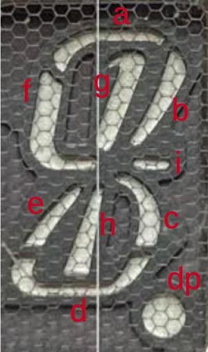
The desktop QT-8D calculator uses an unusual 9-segment display with curved segments, while the handheld EL-8 used an 8-segment display (omitting segment i, which provided a tail on the 4). These produce curved digits, unlike the blocky 7-segment digits seen in most calculators. The zero is particularly unusual: it is half-height. The calculator doesn't suppress leading zeroes, so the half-height zeros are less obtrusive. (1234, for instance, appears as oooo1234.)
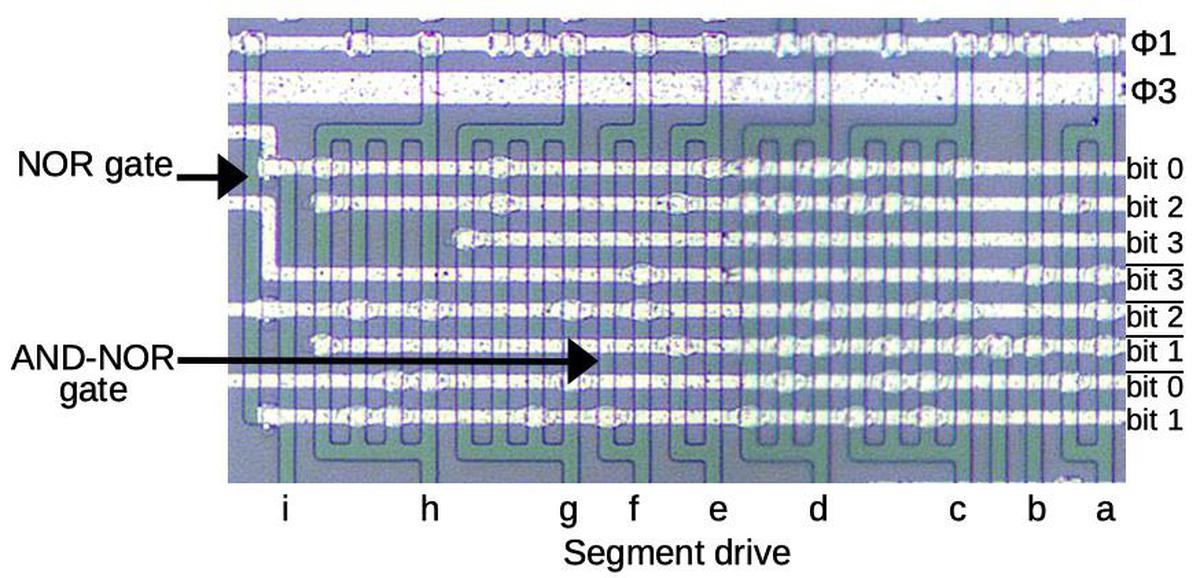
The role of the segment decoder is to take a binary value and drive the appropriate segments, labeled a through i. The circuit below is the interesting part of the decoder circuit. The bit values and their complements enter on the right from the shift register. Most of the segments are decoded by AND-NOR gates; an AND-NOR gate consists of several AND terms with the results NOR'd together. An AND-NOR gate is implemented in four-phase logic as a single gate with a separate vertical strip for each AND term. The strips are tied together at the top and bottom so if any strip is activated, the gate is discharged; this provides the NOR action. As a result, the physical structure of the gate maps directly to its logical structure.
The gate for segment f is indicated on the diagram by an arrow. It has two vertical strips, so two AND terms. Studying the transistor connections, this gate implements: bit1 NOR (bit3 AND bit2). Evaluating this expression shows that f will be active for the digits 4, 5, 8, and 9. Looking at the display, you can verify that these are the digits that use segment f. Similar expressions are used to generate the other segments. For instance, segment h has four AND terms.
Segment i is activated by a NOR gate, which has two parallel vertical segments with three transistors in between. If any transistor is activated, it will connect the segments and discharge the gate, providing the NOR action. NOR gates are rare on the chip, probably because they require twice the width of a NAND gate. Segment i is NOR(bit0, bit2, bit1), so it is activated only for the number 4; this segment provides a short tail on the displayed 4.
Decimal point decoding
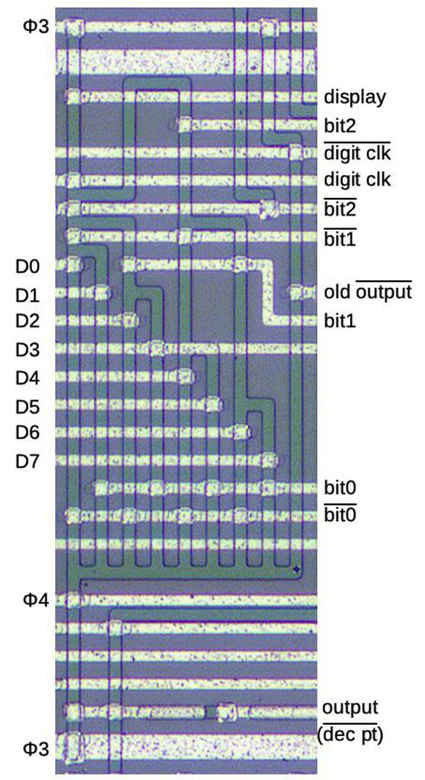
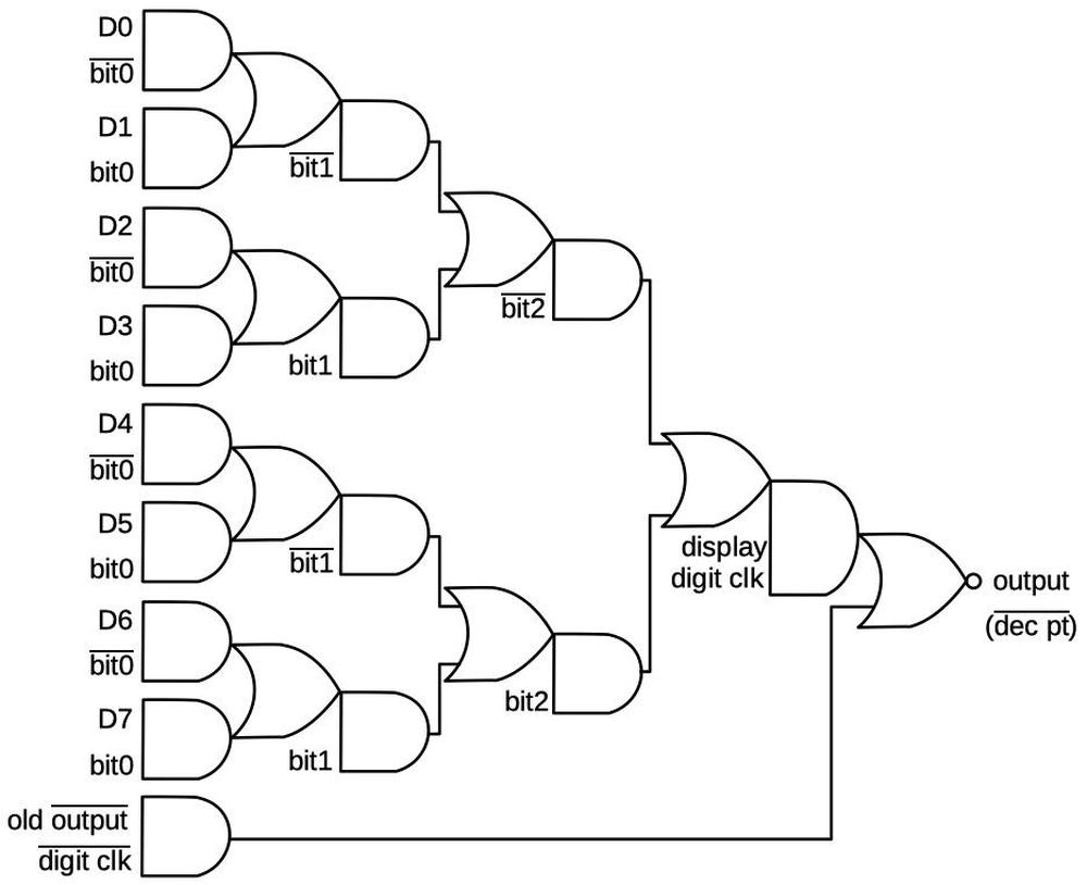
One of the tasks of this chip is to display the decimal point, which is more complex than you might expect. The decimal point is encoded as a 4-bit value, transmitted serially to the chip. Three bits indicate the position of the decimal point (0 to 7), while the fourth bit enables or disables the decimal point. A shift register (described earlier) converts the serial bits to a 4-bit value. A remarkably complex gate (below) is used to determine when the active digit matches the specified decimal point position. At that time, the decimal point segment is activated, causing the correct decimal point to light up.
The circuit is implemented in four-phase logic as a single gate. The gate can be viewed as an 8-to-1 multiplexer that selects one of the eight digit (D) lines based on the bit value. This gate also includes a latch to hold the multiplexed value. Note that if the digit clock is 0, the AND gate at the bottom will cycle the output value (through an inverter, not shown), holding the value. When the digit clock is 1 (i.e. a digit has been read in), a new value from the multiplexer tree will be read. The branching tree structure is visible in the silicon structures above.
Other circuits
I won't describe the remainder of the circuits on the chip in detail. They were implemented using similar techniques, in particular shift registers. The keypress is converted to serial data with a latch and shift register, built from AND-NOR gates. The digit scan circuit is also a latch and shift register, with a gate to start a 1 value. This shift register is triggered by teh digit clock, so it shifts every 4 cycles. The circuit that divides the clock by 4 is a shift register to count four cycles.
Conclusion
Although Sharp managed to fit the calculator circuitry onto five chips, it was soon overshadowed by single-chip calculators. In a few years, calculators shrank from the handheld but blocky Sharp EL-8 to credit-card-sized. The calculator market was highly profitable for a short time until the "calculator wars" caused calculator prices to drop from hundreds of dollars to a few dollars. Most of the hundreds of calculator manufacturers left the market, leaving Texas Instruments, Hewlett-Packard, Sharp, and Casio as the dominant manufacturers.
As for four-phase logic, its success peaked in the 1970s. Most notably, the company Four-Phase Systems created a 24-bit desktop computer in 1971 using four-phase logic, and Motorola bought the company in 1982. For the most part, though, microprocessors of the 1970s used static NMOS logic rather than four-phase logic. I haven't been able to find an explanation of why four-phase logic wasn't more widely used. My suspicion is that improvements in semiconductor technology in the early 1970s reduced the benefits of four-phase logic, specifically the introduction of depletion-load NMOS logic.
I plan to analyze the remaining three calculator chips so follow me on Twitter @kenshirriff for updates. I also have an RSS feed. Thanks to François Gueissaz for doing all the hard work of obtaining the calculator ICs, decapping them, and providing me with die photos and other information.
Notes and references
-
The advantages of four-phase logic are discussed in a talk by Lee Boysel, an early proponent of MOS circuitry and four-phase logic. He founded the company Four-Phase Systems, which build a powerful desktop computer using four-phase logic. His interesting video on MOS history is here. ↩
-
The calculator display uses vacuum fluorescent display (VFD) tubes, developed as a lower-cost alternative to Nixie tubes to avoid paying patent royalties to Burroughs. Nixie tubes are similar to neon bulbs; there are 10 cathodes, each shaped like a digit, and applying 170 volts to a cathode causes the digit to light up with a neon glow.
The multi-segment VFD was invented in 1967 by Noritake Itron Corp. VFD tubes are vacuum tubes, sort of a cross between a triode and a low-voltage CRT. Unlike the "cold cathode" of Nixie tubes, the VFD's cathode is heated, causing electrons to boil off. These electrons are accelerated toward an anode by applying 25 volts to the anode, and cause a phosphor to light up when they hit the anode. A grid between the cathode and anode controls the electron flow; this is how a single tube is selected for multiplexing. The voltage in a VFD is much lower than a CRT, 25 volts instead of 25,000 volts. Another difference is that a CRT deflects the electron beam with deflection coils to create a pattern on the screen, while the VFD uses individual anodes that light up separately for each segment.
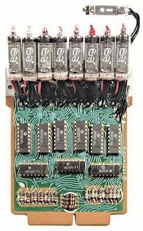
These Sharp calculators were the first calculators to use VFD tubes. The EL-8 calculator uses eight-segment Itron type DG10L tubes while the QT-8D calculator uses nine-segment DG10B tubes. The driver board has nine driver integrated circuits to interface between the calculator chips and the display tubes. ↩
-
I'm skipping over a bunch of details of the calculator. For instance, some signals are active-high, while others are active-low, and some signals are shifted by half a clock. (The design is optimized to minimize the hardware, rather than being conceptually clean.) In this blog post, I'm describing the concepts of the circuitry rather than the cycle-exact details. ↩
-
I haven't found many publications explaining four-phase logic. One is the article Four-phase logic is practical (1977). The 1969 master's thesis Basic design of MOSFET, four-phase, digital integrated circuits has a lot of information. The book MOS integrated circuits and their applications (1970) has a chapter on four-phase logic. See also Low-power VLSI implementation by NMOS 4-phase dynamic logic, published at the surprisingly late date of 2000. ↩
-
Note that the gate is powered only by the clock; there are no power or ground connections. Although the four-phase gate are powered through the clock, the chip does have connections for power (-25V) and ground. Power and ground are used by the output pins so they can provide static signals with more substantial current. Ground is also used for the gate capacitors. ↩
-
Most of the classic 1970's microprocessors used a two-phase clock. They used dynamic circuitry, typically for temporary data storage and timing, but the logic was typically static. The Intel 8086 used dynamic logic in a few places, such as the ALU, probably for performance reasons. ↩
-
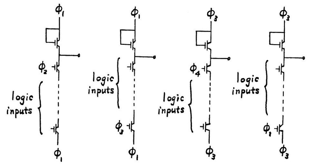
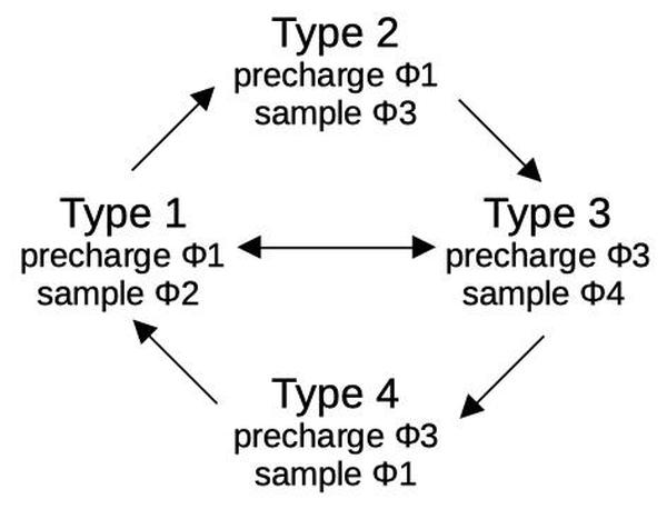
In most cases, four-phase circuitry alternates between φ1φ2 gates and φ3φ4 gates. A problem arises, however, if one path to a gate has an odd number of gates and another has an even number of gates. The solution is two more types of gates, one that precharges on phase 1 and samples on phase 3, and one that precharges on phase 3 and samples on phase 1. These gates are slower, but can interface between the earlier two types. Thus, four-phase logic has four types of gates, distinguished by the clock phases they use. Following the simple interconnection rules ensures that the circuit operates correctly.
The four types of four-phase gates are illustrated in A mathematical model characterizing four-phase MOS circuits for logic simulation. (1968) and Four-phase logic is practical (1977). (I'm pretty sure the second article has some errors in Figure 2 though.)
The four types of four-phase gates.From A mathematical model characterizing four-phase MOS circuits for logic simulation.Only certain combinations of four-phase gates can be connected. The diagram below shows that, for instance, the output from a type 1 gate can connect to the input of type 2 or type 3. A typical circuit alternates between Type 1 and Type 3. The calculator chip uses a few Type 2 gates and Type 4, for example when an extra inversion is required.
Connections between four-phase gates must satisfy certain rules.

4 comments:
Great write up as usual Ken. So, if I'm understanding correctly, because of the clocked phasing of the logic, the processing of the data is kind of "serialized" as the bits move from gate to gate synchronized by the clock. I know that static gates have a delay in when the output is valid after an input change, so this isn't dissimilar to that, but it's more discrete I guess. Very interesting indeed.
Four Phase System's computer was rack-mounted, not a desktop. Its performance level was that of minicomputers, higher than that of first and second-gen desktop PCs. Thanks for finding that Boysel video. I didn't know the origins of the company or how it pioneered MOS DRAM. It was fun to hear how Boysel repurposed his old AL1 ALU slices to blow up TI's single-chip microprocessor patent claims; a great hardware and software hack. I don't think I ever heard him speak personally.
Very interesting.
Four phase logic is actually making a resurgence in modern computing. With PCIe gen6 using it (Quaternary logic) and 4 layer NAND in SSDs.
The curved PWB traces indicate that the layout was done by hand.
One method was to lay down a precise width tape on transparent Mylar sheet to produce a positive representation of the PWB layout. This was the origin of the term "taping" PWB layouts.
Another possibility is that the layout was done using a two layer Mylar film where the opaque layer (it was red and opaque to blue light) was cut using paired knife blades and the part to be the trace removed leaving the transparent lower layer behind. This produced a negative that was then used to expose the trace pattern on a resist-coated copper clad substrate (glass epoxy board, phenolic board, etc.).
Printed wiring board layout folks were artists and magicians to be able to fit what they did into sometimes very limited space, especially if they were limited to only one or two layers.
Post a Comment