Back in the late 1970s, the most popular memory chip was Mostek's MK4116, holding a whopping (for the time) 16 kilobits. It provided storage for computers such as the Apple II, TRS-80, ZX Spectrum, Commodore PET, IBM PC, and Xerox Alto as well as video games such as Defender and Missile Command. To see how the chip is implemented I opened one up and reverse-engineered it. I expected the circuitry to be similar to other chips of the era, using standard NMOS gates, but it was much more complex than I expected, built from low-power dynamic logic. The MK4116 also used advanced manufacturing processes to fit 16,384 high-density memory cells on the chip.12
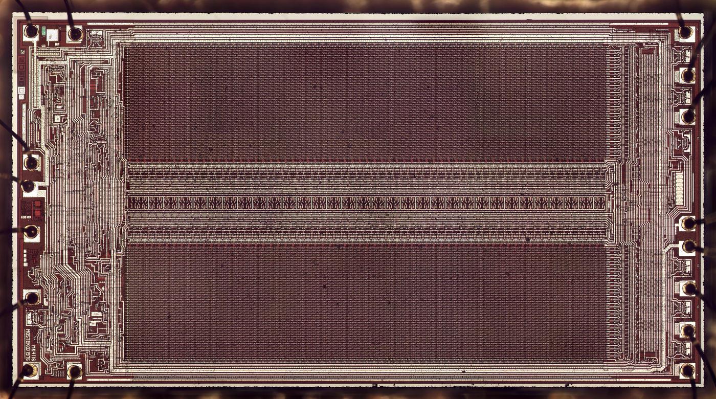
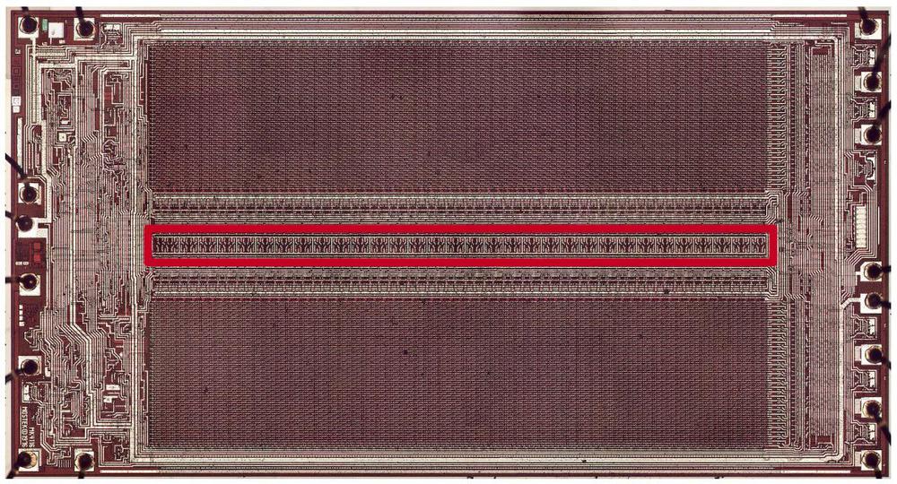
I created the die photo below from multiple microscope images. The white lines are the metal wiring on top of the chip, while the silicon underneath appears dark red. The two large rectangular regions are the 16,384 memory cells, arranged as a 128×128 matrix split in two. In between the two memory arrays are the amplifiers and selection circuits. The control and interface circuitry is at the left and right, connected to the external pins via tiny bond wires.
In dynamic RAM, each bit is stored in a capacitor with the bit's value, 0 or 1, represented by the voltage on the capacitor.3 The advantage of dynamic RAM is that each memory cell is very small, so a lot of data can be stored on one chip.4 The downside of dynamic RAM is that the charge on a capacitor leaks away after a few milliseconds. To avoid losing data, dynamic RAM must be constantly refreshed: bits are read from the capacitors, amplified, and then written back to the capacitors. For the MK4116, all the data must be refreshed every two milliseconds.
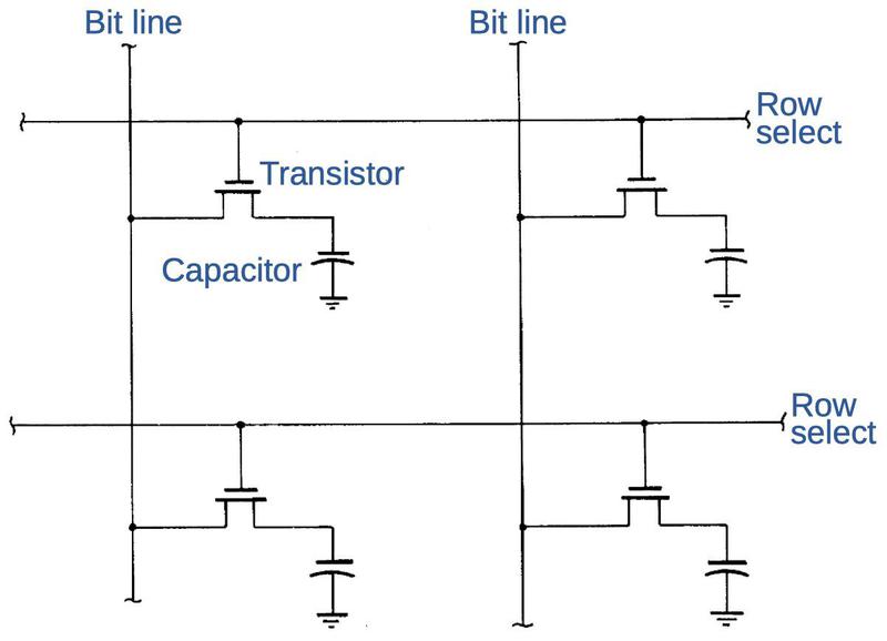
The diagram below illustrates four of the 16,384 memory cells. Each memory cell has a capacitor, along with a transistor that connects the capacitor to the associated bit line. To read or write data, a row select line is energized, turning on the transistors in that row. The row's capacitors are connected to the bit lines, allowing the bits in that row to be accessed.
One of Mostek's key innovations was to multiplex the address pins.6 Earlier memory chips used a separate pin for each address bit; as memory sizes increased, so did the number of address pins. This forced Intel's 4096-bit memory chip, for instance, to use a large, more costly 22-pin package.5 Mostek cut the number of address pins in half by using each address pin twice, first for a "row" address, and then a "column" address. This approach became the industry standard, allowing memory chips to fit into inexpensive 16-pin packages.
Externally, the chip stores a single bit for 16,384 different addresses. (Typically, eight of these chips were used in parallel to store bytes.) Internally, however, the chip is implemented as a 128×128 matrix of storage cells. The row address selects a row of 128 cells7 and then the column address selects one of these 128 cells to read or write.8 Meanwhile, the entire row of 128 cells is refreshed by amplifying the signals and storing them back in the capacitors.
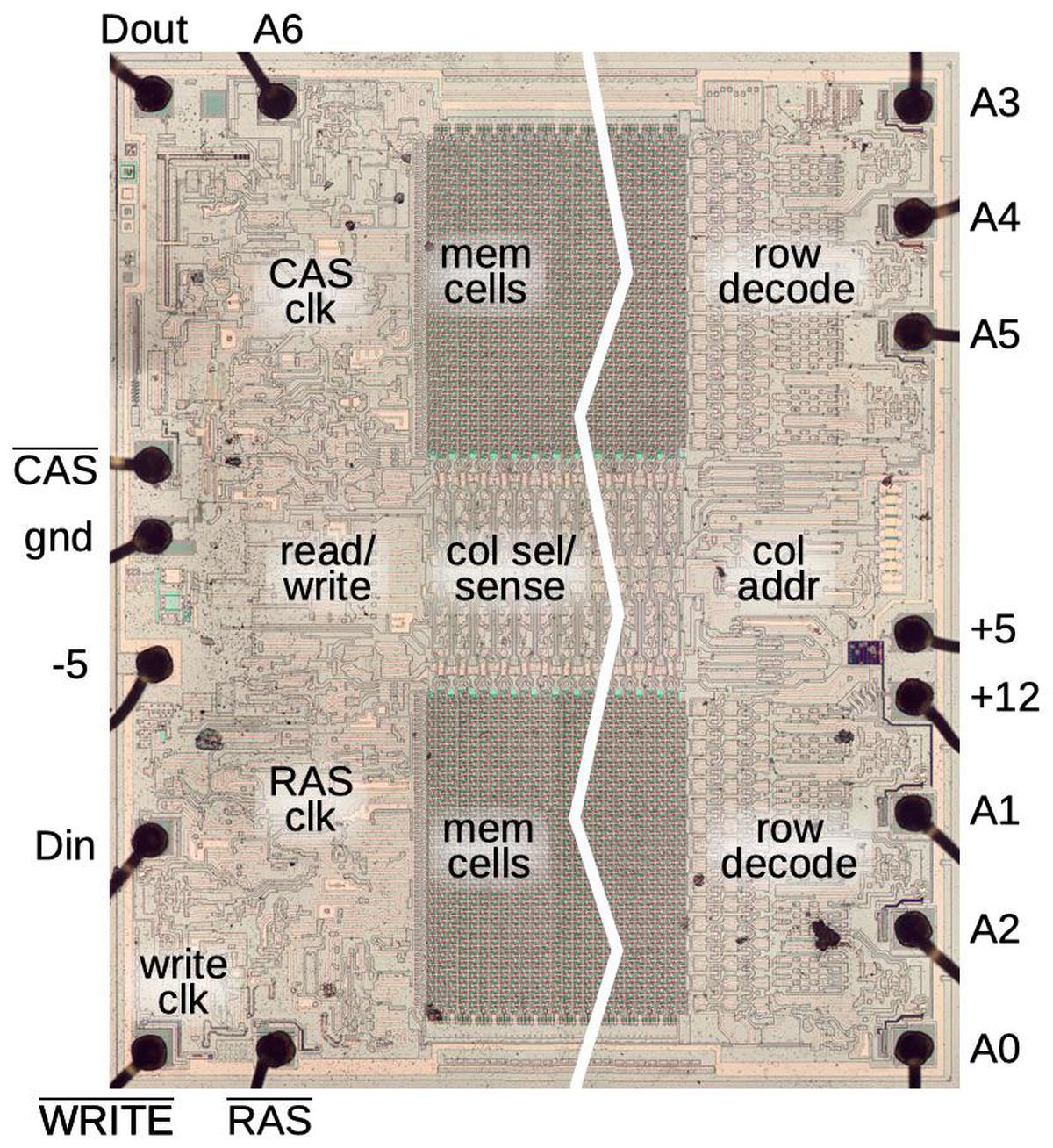
The die image above is labeled with the main functional blocks.9 The chip's 16 pins are labeled around the perimeter,10 including the seven address pins (A0-A6). The Row Address Strobe pin (RAS) is used to indicate the row address is ready, while the Column Address Strobe pin (CAS) indicates that the column address is ready. The two memory arrays are in the center; I've cut out most of the cells to keep the diagram compact. The column select circuitry and sense amplifiers are between the two memory arrays. At the right, the row decode circuitry selects a row based on the address pins, while the column address circuitry buffers the address for the column select circuitry. At the left, the clock circuits generate the chip's timing pulses, triggered by the RAS, CAS, and WRITE pins. Finally, the Data Out and Data In pins provide access to the selected data bit.
Memory cell structure
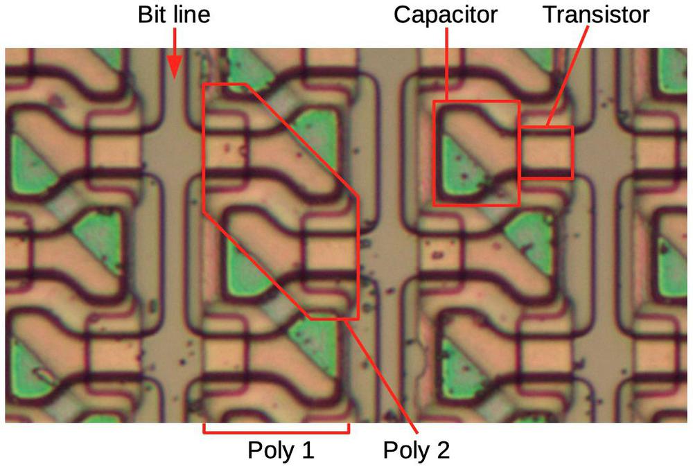
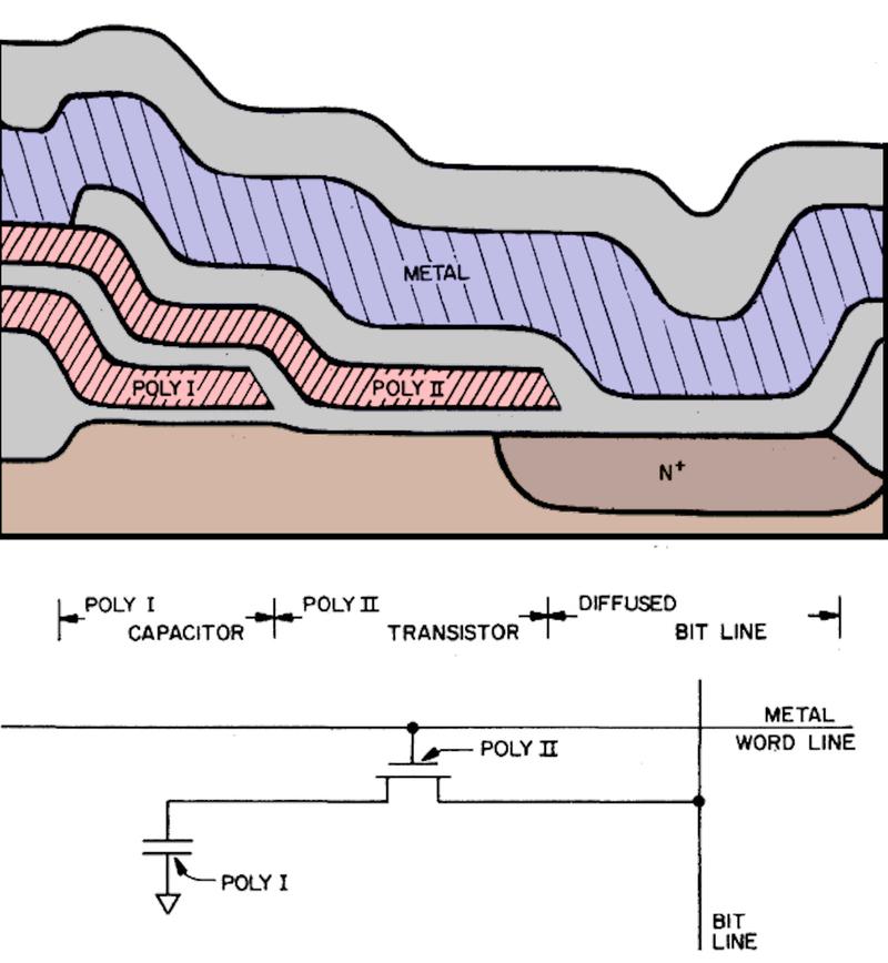
The key to the DRAM chip is the memory storage cell, designed to be as compact as possible. The highly magnified photo below shows some of the storage cells, densely packed together. It's a bit hard to visualize what's going on because the chip is constructed from multiple layers. The bottom layer is the grayish silicon die. On top of the silicon are two layers of polysilicon, a special type of deposited silicon used for transistor gates, capacitors, and wiring. The top layer of the chip is the metal wiring, which was removed for this photo. The photo shows three bit lines in the silicon, with bulb-shaped storage cells connected on either side. Vertical strips of polysilicon (poly 1) over the storage cells implement capacitors: the silicon forms the lower plate, while the polysilicon forms the upper plate. The second layer of polysilicon (poly 2) is arranged in diagonal regions to implement the selection transistors, where square notches in the poly 1 layer allow the poly 2 layer to approach the silicon.
The cross-section diagram below shows the three-dimensional, layered structure of a memory cell. At the bottom is the silicon (brown); the bit line (dark brown) is made from doped silicon. Above the silicon are the two polysilicon layers (red) and the metal layer (purple), separated by insulating silicon dioxide (gray). At the far left, the poly 1 layer and underlying silicon form a capacitor. In between the capacitor and the bit line, the poly 2 layer forms the gate of the transistor. At the left, the poly 2 layer is connected to the metal of the word line, which turns the transistor on, connecting the capacitor to the bit line.
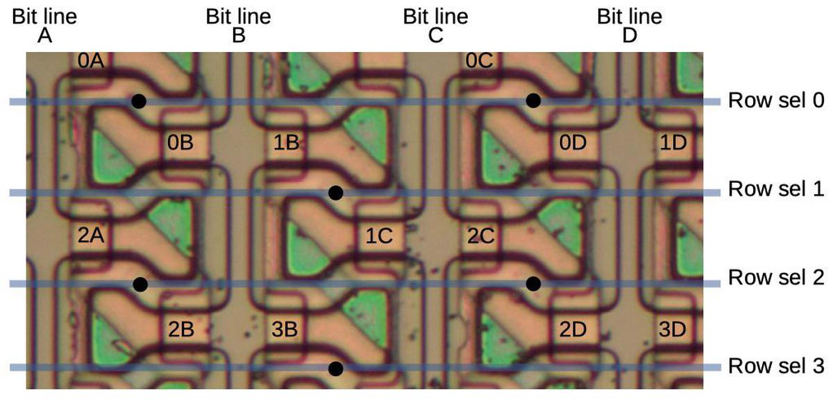
The diagram below illustrates how bits are addressed in the storage matrix. The arrangement is somewhat confusing because columns of cells are offset and interlocked like zippers. A row select line is connected to the centers of diagonal poly 2 regions, so each region controls two transistors on neighboring bit lines. (For instance, in the upper left, the poly region connected to row select 0 forms transistors 0A and 0B.) The result is that each row select line activates 128 cells, one for each bit line in a staggered arrangement.
Low-power circuitry
A key feature of the MK4116 memory chip is that it uses almost no power when it is sitting idle. Although it consumes 462 milliwatts when active, it uses just 20 milliwatts in standby mode. Although low-power circuitry is straightforward to build with modern CMOS technology, the 4116 used earlier NMOS transistors. Most NMOS integrated circuits constructed logic gates with load transistors, a simple technique with the disadvantage of wasting power. Instead, the MK4116 memory chip uses dynamic logic, which is considerably more complex but saves power while idle.
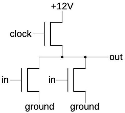
A typical dynamic logic gate (below) operates in two phases. In the first phase, a clock signal turns on the upper transistor, precharging the output to +12 volts, the "1" state. The upper transistor then turns off, but the output remains high due to the capacitance of the wire. In the second phase, the lower transistors can pull the output low. In particular, if either input is 1, the corresponding transistor turns on and pulls the output low, so the circuit implements a NOR gate. This circuit doesn't consume any static power, just a small current to charge the wire capacitance when switching. (The inputs must be carefully timed so they don't overlap with the precharge clock.) The use of dynamic circuitry makes the 4116 much more complex than it would be otherwise since the gates are controlled by clock signals, which need to be generated.
The row select circuitry
The purpose of the row-select circuitry is to decode the 7 address bits and energize the corresponding row select line (out of 128) to read one row of memory. In the first step, 32 5-input NOR gates decode address bits A0 through A4. These NOR gates are implemented in the compact circuit shown below. Each NOR gate takes a different combination of non-inverted and inverted address bits and matches a particular 5-bit address. These NOR gates use dynamic logic, first pulled high and then discharged to ground, except for the selected address which remains high. Next, each NOR output is split into four, based on A5 and A6. The result is that one of 128 row select lines is activated, turning on the transistors for that row in the matrix.
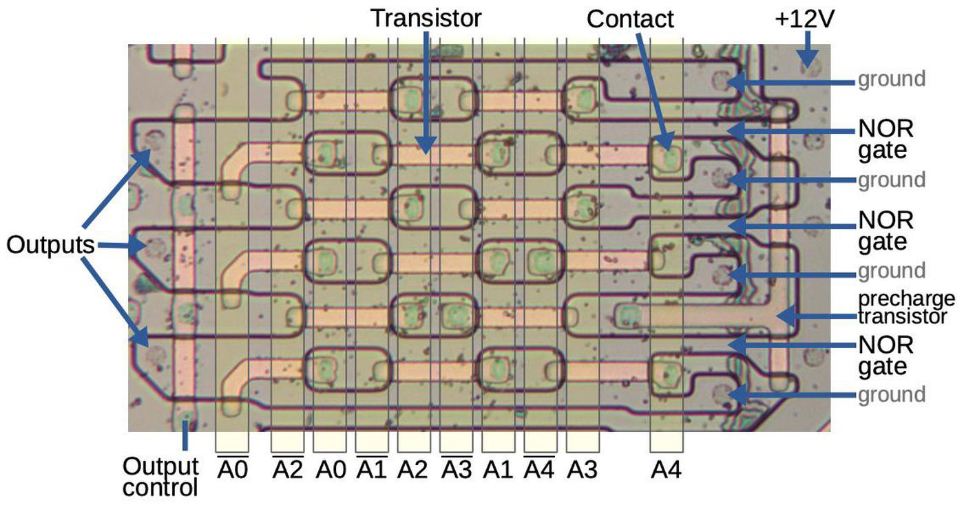
The NOR gates are implemented in several compact blocks; one block of three NOR gates is shown below. Each NOR gate is a horizontal stripe of doped silicon, with ground above and below it. Each NOR gate has transistors (pink stripes) connected to ground alternating above and below it. A transistor will pull the NOR gate low if the connected address line is high. The precharge transistors at the left pull the NOR gates to +12 volts, while the output control transistors control the flow of the decoded outputs to the rest of the circuitry.
The small greenish blobs at the end of a transistor gate (pink stripe) are connections (vias) between a transistor gate and an address line. The address lines are represented as vertical yellow stripes (since the metal layer was removed). Note that each transistor gate has an address line at the right and the inverted address line at the left; thus, the NOR gates all have the same basic layout, but with the contacts changed to match a particular address. For instance, the upper NOR gate has transistors connected to A0, A2, A1, A3, and A4, so it will be active for address 00000; any other address will pull it low.
The sense amplifiers
The sense amplifiers are one of the most challenging parts of designing a memory chip. The job of the sense amplifier is to take the tiny voltage from a capacitor and amplify it into a binary 0 or 1.11 The challenge is that even though 12 volts is stored in a capacitor, the signal from the capacitor is very small, is only 100 millivolts or so. (Because the bit line is much larger than the tiny memory cell capacitor, the capacitor causes a very small voltage swing.)12 It is critically important for the sense amplifier to operate accurately, even in the presence of noise or voltage fluctuations, because any error will corrupt the data. The sense amplifier circuit must also be compact and low power since there are 128 sense amplifiers.
The chip's 128 sense amplifiers, one for each column, are located between the two memory arrays as shown above. During a read, 128 values in a row are accessed in parallel and amplified by the sense amplifiers. These 128 values are then written back to refresh the values in the capacitor. For a write operation, one of the bits is updated with the new value before they are written back.
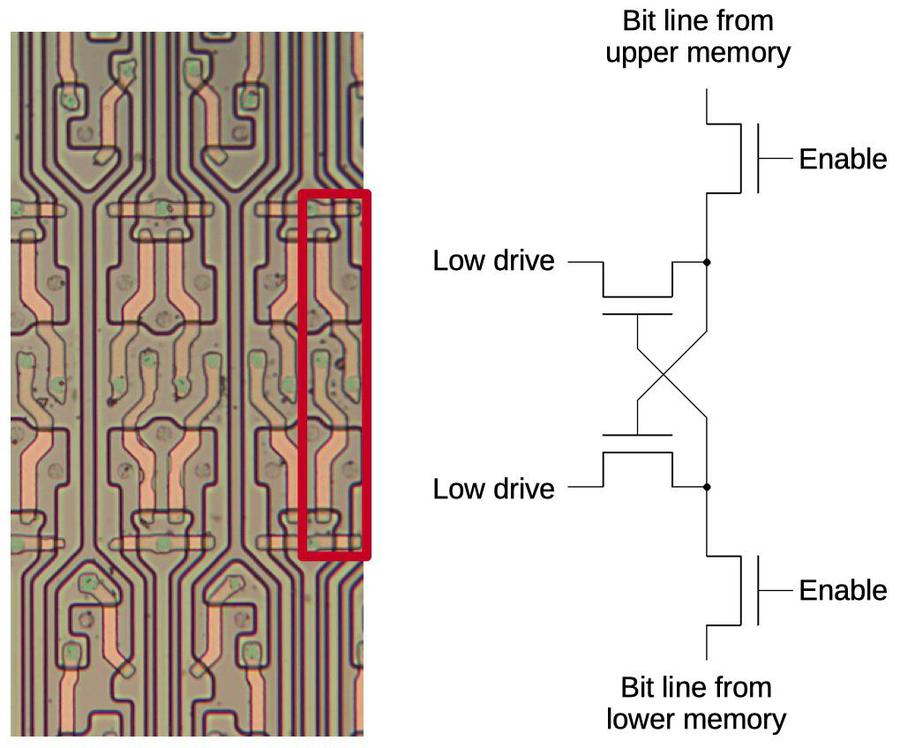
Each sense amplifier (above) is a very simple circuit. It takes two inputs and compares them, pulling the lower one to 0.13 It is built from two cross-coupled transistors, each trying to pull the other one low. Whichever transistor has the higher voltage to start with will "win", forcing the other side low.14 The sense amplifier is sensitive to very small voltage differentials, allowing it to distinguish the small signals from a storage cell.
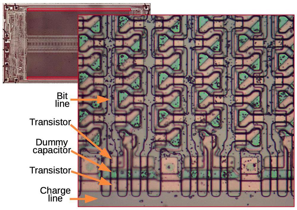
Locating the sense amplifiers between the two memory arrays isn't arbitrary, but the key to their operation: this is the "divided bit line" architecture introduced in 1972. The idea is that one input to the sense amp is the voltage from the desired memory cell, while the other input is a threshold voltage from a "dummy cell" in the opposite memory array. Dummy cells are constructed and precharged like real memory cells except the capacitor is half-sized, so they provide a voltage midway between a 0 bit and a 1 bit.3 If the voltage from the real memory cell is lower, the sense amp outputs a 0, and if higher, it outputs a 1.
The dummy cells are located on the edges of the memory arrays, as shown above. They consist of capacitors and transistors (similar to real memory cells), but with a separate line to charge them. The advantage of the dummy cell approach is that manufacturing differences or fluctuations during operation will (hopefully) affect the real cells and dummy cells equally, so the voltage from the dummy cell will remain at the correct level to distinguish beween a 0 and a 1. Address bit A0 controls which half of the array provides real data to the bit lines and which half connects dummy cells to the bit lines.
The column select circuitry
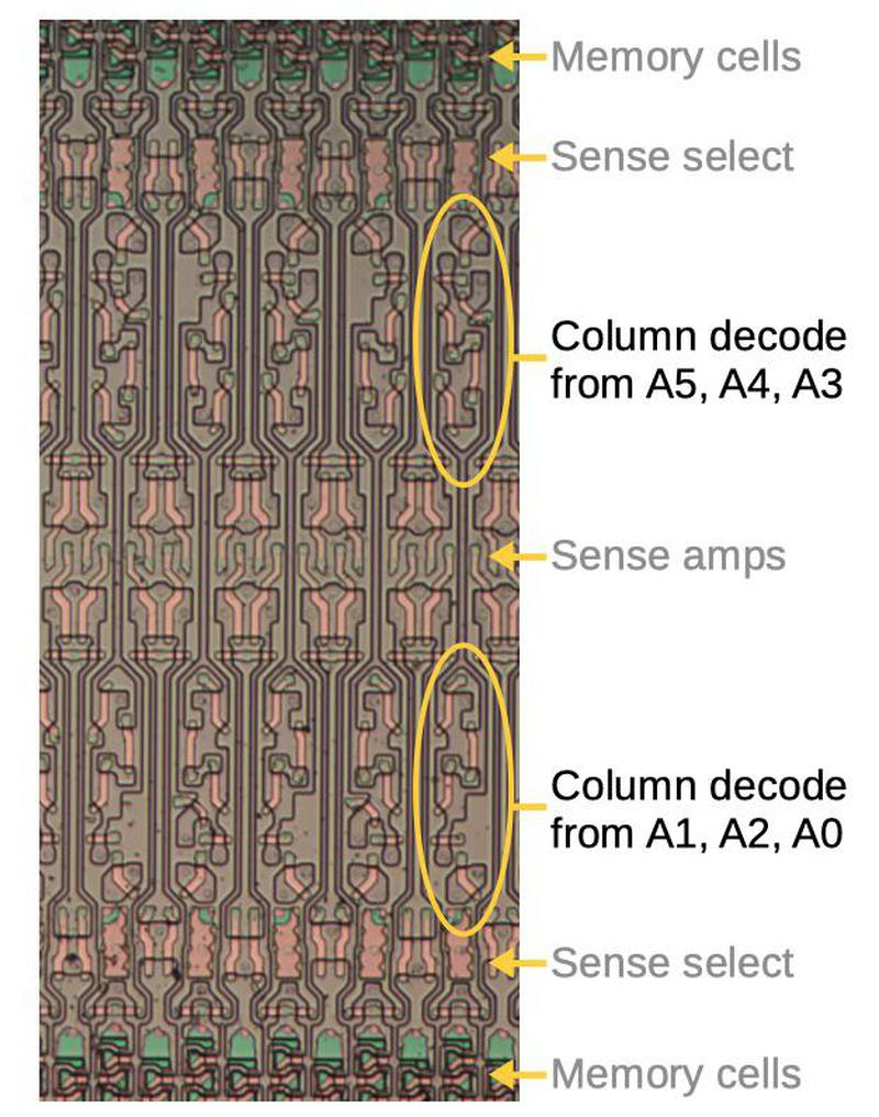
The purpose of the column select circuitry is to select one column out of the 128-bit row; this is the bit that is read or written. Each column select circuit is twice as wide as a memory cell, so they only decode one of 64 columns. The result is that two bits are selected at a time, and circuitry elsewhere selects one of the two bits. Like the row select circuitry, the column select circuitry is implemented by numerous NOR gates, each matching one address. For column select address bits A0 through A5 select one of 64 lines, selecting two columns at a time. These two bit lines are connected to data lines transmitting the signals to the I/O circuitry. (Since the bit lines for the upper and lower halves of the matrix are separate, there are actually four bit lines selected by the column select circuit.) As with the row select circuitry, dynamic logic is used, controlled by various timing signals. Note that each NOR gate is physically split into two parts with the sense amp in the middle.
Footnote 15
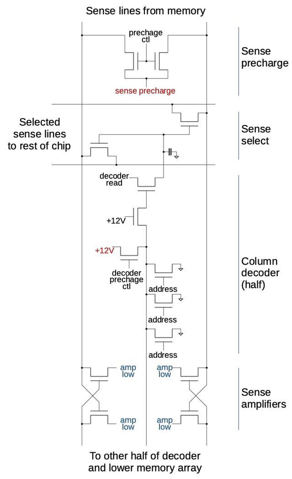
The schematic below shows how the column decoder works with the sense amplifier. The diagram shows two bit lines and the top half of the column decoder and sense circuitry; it is mirrored for the lower array. At the top, the sense precharge circuit pulls all the bit lines high. At the bottom, the sense amplifiers amplify and refresh the signals as explained above. The column decoder matches a particular 6-bit address, so one of the 64 decoders will activate the associated sense select circuit, connecting the chip's I/O circuitry to four bit lines (two from the upper memory array as shown here and two from the lower memory array).
At this point, four bit lines have been selected for use and their signals are passed to the input/output circuitry; the column select circuitry only decoded 1-of-64, while there are 128 columns, and each half of the array has separate bit lines. Column address bit A6 provides the final selection between the two columns. The selected bit is sent to the data-out pin for a read. For a write, the value on the data-in pin is sent back through the appropriate wire to overwrite the value in the sense amplifier. This circuitry is implemented using dynamic logic and latches, controlled by various timing signals. Much of the circuitry is duplicated, with one copy for the upper half of the memory array and one copy for the lower half. Row address bit A0 distinguishes which half of the matrix is active and which half is providing dummy data). (Note that row address bit A0 was already used to select a particular row, but the circuitry has "lost track" of which was the real row and which was the dummy row, so it must make the selection again.)
Clock generation
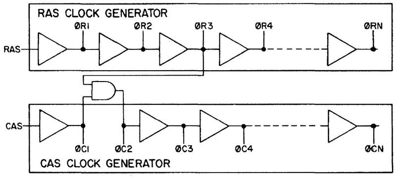
The chip requires many timing signals for the various steps in a memory operations. The memory chip doesn't use an external clock, unlike a CPU, but generates its own timing signals internally. The diagram below illustrates the clock generators, using buffers to create a delay between each successive clock output. The first set of timing signals is triggered by the row-access strobe (RAS), indicating that the computer has put the row address on the address pins. The next set of timing signals is triggered by the column-access strobe (CAS), indicating the column address is on the address pins. Other timing signals are triggered by the WRITE pin.
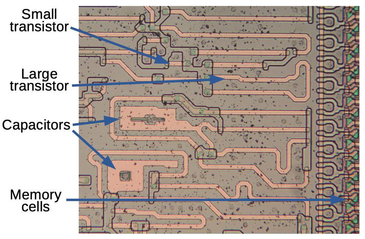
The real clock circuitry is much more complex than the diagram indicates, consisting of dozens of transistors in multiple chains, feeding back in complex ways to shape the pulses. (Among other things, using dynamic logic requires each buffer to have both an input that pulls it high and an input that pulls it low, forming almost a circular problem.) These gates are mostly built from large transistors, as shown below, to provide enough current to drive the circuitry, and to increase the gate delay sufficiently. The clock circuitry also uses many capacitors, probably bootstrap loads to pull signals up sharper. I'm not going to describe the clocks in detail since it's a complicated mess.
Input pins
The chip uses surprisingly complex circuits for the address pins and the data input pin. Mostek's earlier memory chip had problems due to noise margins on the inputs, so the MK4116 uses a complex circuit with an analog threshold, capacitor drive, and multiple controls and latches.
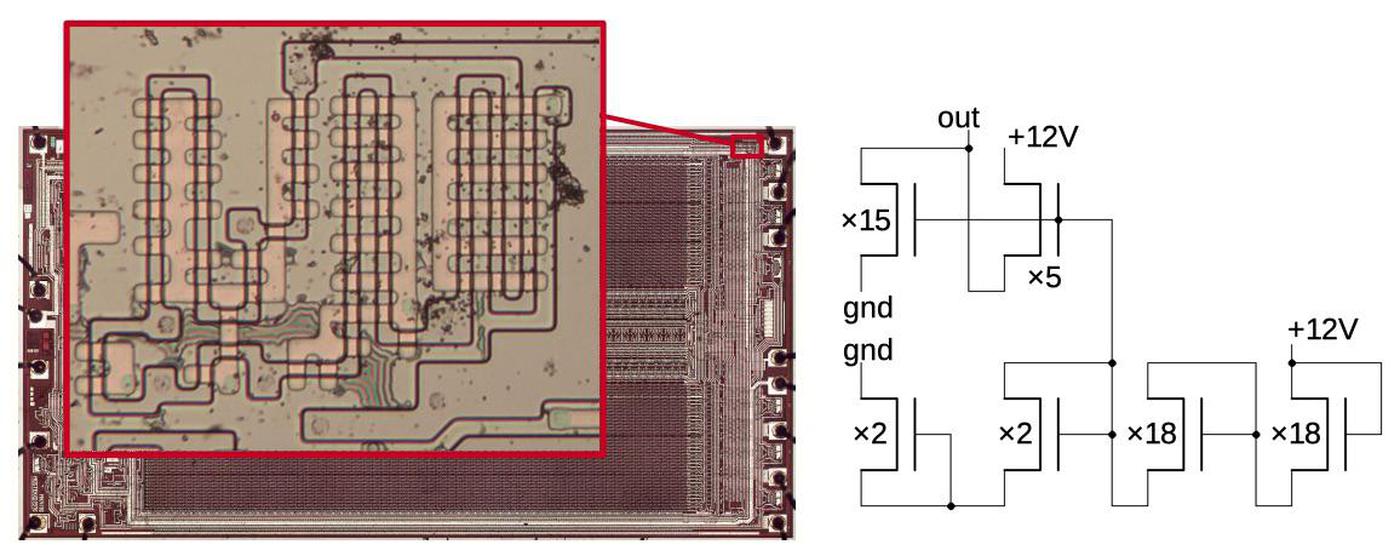
The diagram below shows the threshold generation circuit, which generates a 1.5-volt reference. It uses many tiny transistors in series to generate the voltage level. Conceptually, it is similar to a resistor divider between power and ground to produce an output voltage. However, resistors are both power-hungry and difficult to build in integrated circuits, so transistors are used instead. Since this circuit is always active, the designers needed to minimize its current; this was achieved by using many transistors in series.
The voltage on the input pin and the threshold voltage are fed into a differential amplifier/comparator, conceptually similar to the sense amplifiers. Each side tries to pull the other side low, ending up with a 1 for the "winning" side and 0 for the "losing" side. Thus, the input is converted into a binary value. The result from the comparator is stored in a latch. Multiple timing signals gate the input signal, precharge the circuitry, and control the latch.
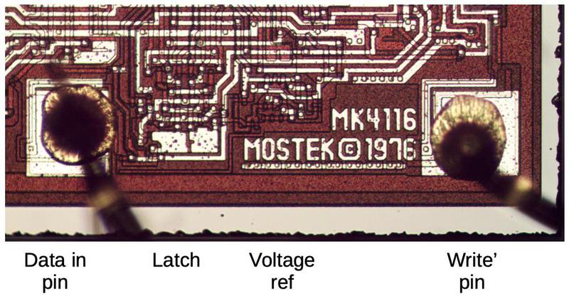
The photo above shows the input circuit for the data-in pin. Next to the pin's bond wire is the threshold circuit and latch; the two capacitors are the large rectangles of metal. The voltage reference circuit is next; the data-in voltage reference is similar to the address voltage reference described above. (I left the metal layer on for this photo; the polysilicon and silicon underneath is obscured by the oxide layer.)
Conclusion
This memory chip was much more complex than I expected. I studied a simple Intel memory chip earlier so I assumed this DRAM would be larger but not much more complicated. Instead, the MK4116 has complex circuitry with over 1000 transistors controlling it, in addition to the 16,384 transistors for the memory cells and about 1500 transistors for the column selects and sense amps. A cause of the complexity is that the design needed to optimize multiple axes: density, speed, and power efficiency.16
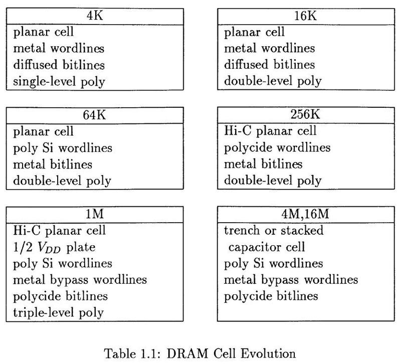
The table below shows that each generation of DRAM chips required substantial technological changes and new developments. Memory designers don't just sit around waiting for Moore's Law to increase the memory capacity; they have to constantly develop new techniques because DRAM storage cells are fundamentally analog. Fortunately, DRAM designers have continued to solve memory scaling problems; 16-gigabit DRAMs recently went into production, an amazing factor of a million larger than the 16-kilobit MK4116 DRAM chip of 1976.
I announce my latest blog posts on Twitter, so follow me @kenshirriff or my RSS feed. Thanks to Mike Braden for suggesting the MK4332 chip to me.
Notes and references
-
A brief history of memory innovations is here. For detailed information on DRAM circuits, see this 1990 thesis on sense amplifier design. For history, Storage array and sense/refresh circuit for single-transistor memory cells (1972) introduced the concepts of dummy cells and cross-coupled sense amplifiers. Intel's chip is discussed in A 16 384-Bit Dynamic RAM (1976) while Mostek's chip is discussed in A 16K × 1 bit dynamic RAM (1977) and 16K - The new generation dynamic RAM (1977). Inconveniently, I found most of these references after I had this blog post nearly completed. ↩
-
An unusual characteristic of the chip is that it doesn't use "buried contacts". The issue is how to connect a polysilicon wire to a silicon circuit. In integrated circuits of the 1960s, polysilicon couldn't be connected to silicon directly, so a via connected the polysilicon wire to the metal layer, which had a short connection to a second via that connected down to the silicon. In 1968 at Fairchild, Federico Faggin invented the buried contact, a way to connect the polysilicon and silicon directly. This was much more convenient, so all the NMOS chips that I have examined use buried contacts.
However, the 4116 doesn't use buried contacts. Instead, it uses the obsolete connections through the metal layer. It's a mystery why they did this. Perhaps the metal wiring density was low enough that the additional segments weren't a problem and they could eliminate one masking and processing step. (Another theory is maybe there were patent issues, but I'm not aware of any patent on the buried contact.) But this illustrates that technological progress isn't consistently linear. Even an advanced chip like the 4116 can use obsolete techniques in some areas. ↩
-
In the MK4116, a 0 bit is represented by storing 12 volts on the capacitor, while a 1 bit is represented by 0 volts on the capacitor. This is backward from what you might expect, but probably saved an inverter somewhere in the circuitry. To avoid confusion, I ignore this in the text. ↩↩
-
Early dynamic RAMs such as the Intel 1103 used three transistors per cell and used separate lines for reading and writing data. Improvements in memory technology shrunk the circuit to a single transistor and a single data line. Static RAM, in comparison, often requires 6 transistors per bit, but has the advantage of not needing to be refreshed. ↩
-
For example, Intel's 2107 4096-bit DRAM required 22 pins, as did the 2101 256×4 static RAM chip. It's ironic that Intel used larger packages for these memory chips because a few years earlier, Intel had steadfastly refused to go beyond 16 pins, forcing the Intel 4004 microprocessor to use a 16-pin package. The 8008 microprocessor was barely allowed 18 pins, when 24 pins would have been more convenient. This made the 8008 slower and harder to use. ↩
-
Although multiplexing the address pins might seem trivial, Mostek claims that they bet the company on this idea. The problem is how to implement multiplexing without making memory accesses wait while both parts of the address are loaded. (The time to read memory was a key factor in computer design, so every nanosecond counted.) In Mostek's solution, first the row address is put on the address pins, and the row-access strobe (RAS) is activated. While the chip is reading that row from memory, the computer puts the column address on the address pins and activates the column-access strobe (CAS). By the time the 128 bits of the storage row have been read, the column address is available and the desired bit is selected from the row of 128 bits. In other words, reading of the row is overlapped with loading of the column address, so multiplexing doesn't slow the system. However, careful timing is required to make this multiplexing work; much of the chip is devoted to clock circuitry to generate the necessary timing pulses. ↩
-
The RAM chip operates on memory a row at a time, and then selects one entry from the row. This isn't the obvious way to access memory. In comparison, magnetic core memory also holds memory cells (cores) in a matrix, but accesses a single cell using X and Y select lines. A key reason for a DRAM to operate a row at a time is so the entire row can be refreshed at once, dramatically reducing the performance overhead from refresh operations. ↩
-
You might wonder if it's possible to read multiple bits from a row without repeating the entire row-read operation. The chip designers thought of that and provided several techniques to boost efficiency. The page-read and page-write functions let you rapidly access multiple bits in a 128-bit page (i.e. row). A read-modify-write sequence lets you read a row, modify bits in it, and write it back without repeating the row-read. A RAS-only refresh operation lets you read and refresh a row without providing a column address. The point of this is that the chip designers implemented clever features so customers could squeeze as much performance out of their memory system as possible. See the datasheet for details. ↩
-
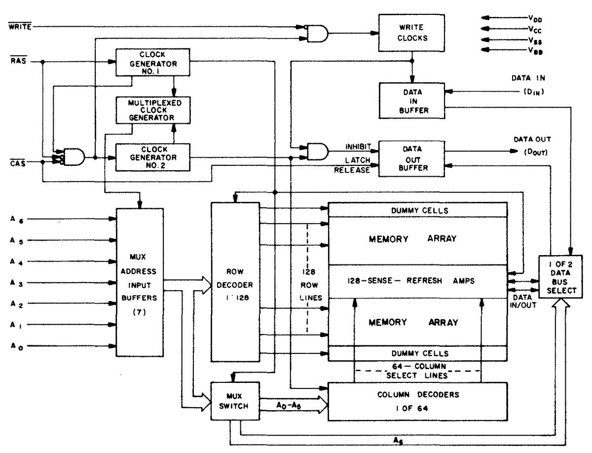
The block diagram below shows the main functional blocks of the 4116. Many parts of this block diagram didn't make sense to me until after I had reverse-engineered the chip, such as the clock generator, dummy cells, and "1 of 2 data bus select". Many datasheets present a somewhat abstracted view of how the chip operates, but the 4116 datasheet accurately matches the implementation.
Block diagram of the 4116 memory chip, from the databook. -
One inconvenient feature of the memory chip is it requires three different voltages: +12 volts, +5 volts, and -5 volts. Almost all the circuitry runs on 12 volts. The 5-volt supply is used only to provide a standard TTL voltage level for the data out pin. The -5 volts is a substrate bias, connected to the underlying silicon die to improve the characteristics of the transistors. Later chips implemented a charge pump circuit to generate the bias voltage, eliminating the need for an external bias voltage. Later memory chips also eliminated the need for +12 volts. This simplified use of the chips, since only a single-voltage power supply was required. A less-obvious benefit is that this made two of the chip's 16 pins available for other uses. Specifically, these pins were used as additional address bits in the next two generations of memory chips, the 64-kilobit and 256-kilobit chips. As a side effect, the address pins are in a somewhat scrambled order, due to the location of the available pins. ↩
-
It's not a coincidence that the input to the sense amp is very small, just enough to be reliably amplified. This is a consequence of economics: if the DRAM produced a large voltage difference, the designers would shrink the cells to save money. But if the voltage difference was too small for reliability, the designers would need to increase the cells. The result is a design where the voltage difference is just barely large enough to be reliably amplified by advanced circuitry. (We noticed the same thing when using a vintage 1960s IBM core memory (video); we were just barely able to read the core values. The cause is the same: if the cores had produced nice clean pulses, they were larger than they needed to be.) ↩
-
When the capacitor is connected to the bit line, the resulting voltage will depend on the relative capacitances of the capacitor and the bit line. The bit line capacitance is said to be 800 fF, while the storage cell has 40 fF capacitance, for a 20:1 ratio. Thus, the resulting voltage will be very close to the +12V precharge voltage on the bit line, but perturbed a few hundred millivolts. ↩
-
The sense amplifier can only pull a signal low, not raise it, so you might wonder where the amplification happens. Both sides are precharged to +12 volts and the memory cell capacitance only pulls the sides down by 100 millivolts or so. The "winning" side will remain very close to 12 volts, while the other side is pulled to 0 by the sense amp. Thus a 1 bit is pulled higher by the precharge, while a 0 bit is pulled lower by the sense amp. ↩
-
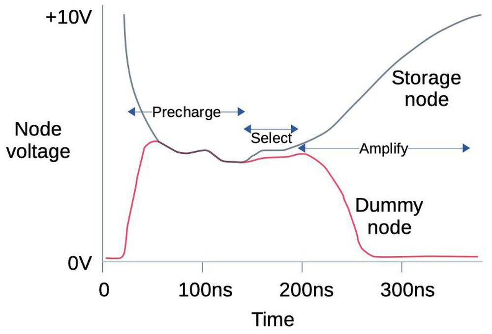
The diagram below shows the sense amplifier voltages during operation of a prototype DRAM sense amp. First, the two sides of the sense amp are precharged to the same voltage. Next, a DRAM storage node is selected on one side and a dummy node on the other. Note that the voltage difference between the two sides is very small, maybe 200 millivolts. Finally, the difference is amplified, forcing the higher side up and the lower side down. In this case, the storage node held a 1 so it started slightly higher. If it held a 0, it would start slightly lower and the two lines would diverge in opposite directions. The point is that the sense amp takes a very small voltage differential and amplifies it into a large binary signal.
Voltage diagram for a prototype sense amp (not the 4116). Based on Storage Array and Sense/Refresh Circuit for Single-Transistor Memory Cells, 1972.One difference between this sense amp and the MK4116 is that this circuit is precharged to a midpoint voltage, while the MK4116's is precharged to +12 volts. In this sense amp, one signal must be pulled high, while in the MK4116 both signals start near +12V and one is forced low. ↩
-
Robert Proebsting, co-founder of Mostek and developer of address multiplexing, has an oral history that provide some information on the 4116. He discusses why the column decoder selects one of 64 columns and the selection between the pair happens earlier. The reason is they wanted the noise from the address lines to be equal on both sides of the sense amp, so they have three address line pairs on each side. ↩
-
Intel produced 16,384-bit DRAM chips before Mostek, the 2116 and others, but Mostek's chips beat Intel in the marketplace. Interestingly, the internal structure was completely different from the MK4116. The 2116 contained four memory arrays internally and was structured as two independent 8-kilobit memories. This saved on power since the unused half could be left unpowered during a memory access. Moreover, if a 2116 chip had a manufacturing flaw in one half, Intel repackaged it as an 8-kilobit 2108 chip with either the upper or lower half operational. The user had to set address bit A6 appropriately to get the working half. ↩
16 comments:
I'm surprised they ran A0-A4 and their complements all the way to the decoders; I had been taught that it was better to predecode A0/A1 and A2/A3 to produce four one-hot signals and reduce the width of the decoder. That reduces both the dynamic power (fewer long lines toggling) and speeds up the decoder by having a narrower gate without increasing the number of wires (4 one-hot instead of 2 complementary). Mind you for dynamic NMOS, wide NOR gates are really cheap so I guess it didn't matter too much.
Excellent post and analysis. A small typo about the Samsung link you provided. It's 16 Gigabit not Gigabyte.
I absolutely love your blog, Ken! I wish my own computer science degree included a course on disassembling old CPUs, in addition to having us design small microcontrollers from scratch. Is there a book/video course on chipset design that you would recommend?
Should the last paragraph refer to 16 gigabit and 16 kilobit rather than -byte?
Ken, great work (as usual). Note 12 seems incomplete, it ends mid-word and there's no full stop.
Brian mentioned the incomplete note 13, but the information is given again in note 13 where it says "100 milivolts or so".
Myst: For old chips, Mead and Conway gives a good overview of VLSI technology. For modern chips, "CMOS VLSI design" gives a reasonable overview. "Modern Processor Design" explains processor architectures well, superscalar and pipelining. Any readers have other recommendations?
Anonymous, DT, Brian, Jecel: thanks for finding my errors; I have fixed them.
I was hired at Mostek in 1980 as a new grad. I worked on processors, primarily the Z80 family, so I didn't work directly with this chip. I had friends that worked on the MK4116, it was a really high volume military grade chip for many years.
Most of us think about DRAM going into personal computers, but at that time the market was mostly mainframe and minicomputers, which had a lot of DRAM chips. Reducing the package size made a huge difference in large computers, not so much in PCs of the day.
Mostek had a training program, I was lucky enough to attend design classes taught by Bob Probstein. He was a very good engineer, also a darn good teacher.
Mostek made the muxed address DRAM an industry standard instead of keeping it proprietary. In those days, more so than today, companies really avoided single sourced components. This is why the MK4116 design changed the industry.
Is there a good reason why DRAM chips have the GND/Vcc connections reversed from what is usually seen with TTL, for example?
Great article as always, thanks.
A fun walk back in time. Thanks! I was thinking back to a particular project, and wondering if Google might yield me any usable chronology. It didn't, but I did find your blog!
Dogzilla and I likely overlapped, as I joined MOSTEK out of college in June 1979. Started in 1215 Crosby, ended up in the South Bldg. I was assigned to Reliability on the MK4116 Rev G', and yes, Bob Probstein was an engineer's engineer.
I still have my 1979 Memory Databook and might even have an old Dick Foss MOSAID reverse engineering / construction analysis report on the G' and earlier revisions buried somewhere.
Wow! Another Mostek "grad" here, also overlapping with Steve and Dogzilla! Like Steve, I also started June 1979 in 1215 Crosby, Fab "B" (I think? That was a long time ago...) and I was actually making 4116s. I was one of the supervisors for the photo-lithograph group and remember seeing ALL of the traces on the wafers above.
Thank you for preserving this!
The "burried contact" link in footnote 2 is a 404
Quite heavy reading at times, fantastic article, I totally zoned out whilst reading it.
reading it. great it, unaware of my surroundings
I am under the impression that many people think the 4116 is failure prone. Was there anything in your investigation or your understanding of the 4116 that would maybe lead them to be more likely to fail over time? A lot of people replace them with later higher density 4164 which is considered more reliable.
https://www.intel-vintage.info/intelmemory.htm has gone to the big cloud in the cloud... IE no longer working. So it's time to replace it with the archival version.
https://web.archive.org/web/20220319073833/https://www.intel-vintage.info/intelmemory.htm
Mostek too offered a half-working 4116, as the MK4108. Users would hold column A0 high or low depending on the chip marking. These were used in Atari's 8K RAM boards for the 800 and 400.
Post a Comment