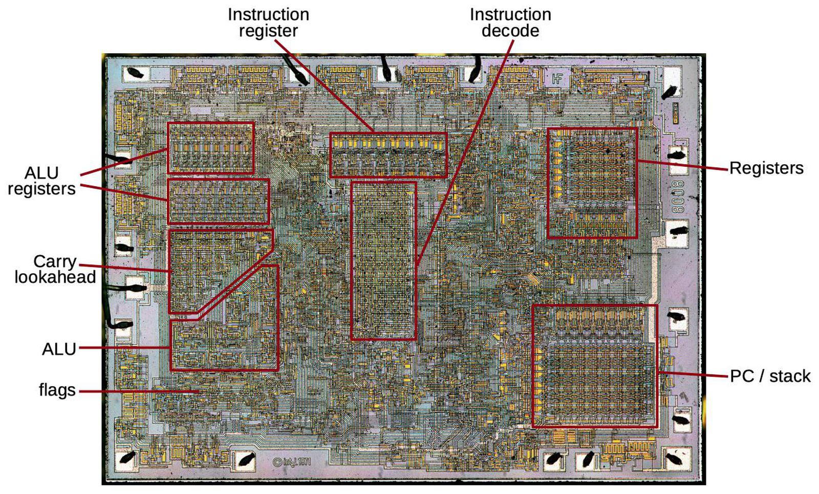
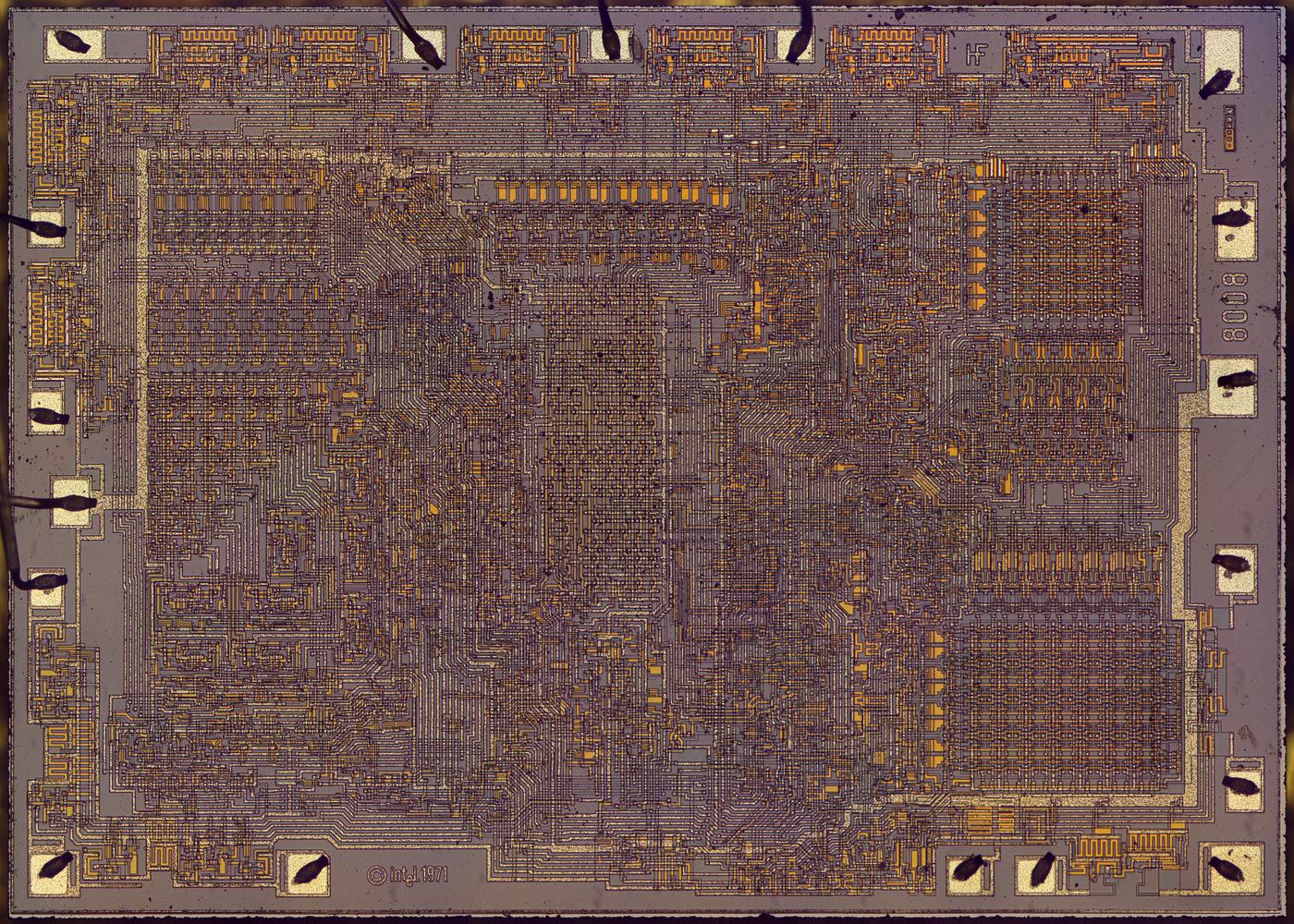
The die photo below shows the main functional blocks1 including the registers, instruction decoder, and on-chip stack storage. The 8-bit arithmetic logic unit (ALU) is on the left. Above the ALU is the carry-lookahead generator, which improves performance by computing the carries for addition, before the addition takes place. It's a bit surprising to see carry lookahead implemented in such an early microprocessor. This blog post explains how the carry circuit is implemented.
Most of what you see in the die photo is the greenish-white wiring of the metal layer on top. Underneath the metal is polysilicon wiring, providing more connections as well as implementing transistors. The chip contains about 3500 tiny transistors, which appear as brighter yellow. The underlying silicon substrate is mostly obscured; it is purplish-gray. Around the edges of the die are 18 rectangular pads; these are connected by tiny bond wires to the external pins of the integrated circuit package (below).
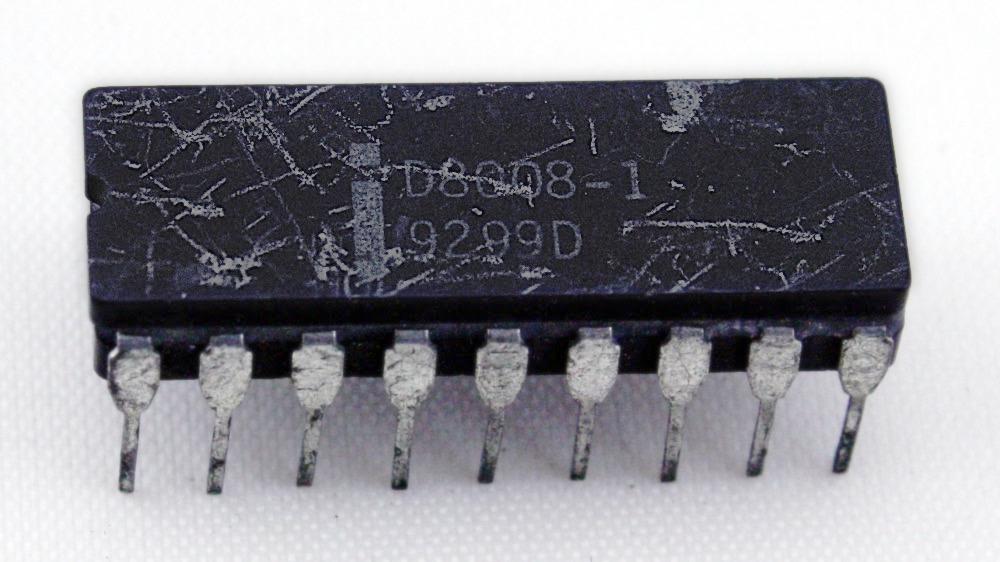
The 8008 was sold as a small 18-pin DIP (dual inline package) integrated circuit. 18 pins is an inconveniently small number of pins for a microprocessor, but Intel was committed to small packages at the time.2 In comparison, other early microprocessors typically used 40 pins, making it much easier to connect the data bus, address bus, control signals, and power to the processor.
Addition
The heart of a processor is the arithmetic-logic unit (ALU), the functional block that performs arithmetic operations (such as addition or subtraction) and logical operations (such as AND, OR, and XOR). Addition was the most challenging operation to implement efficiently because of the need for carries.3
Consider how you add two decimal numbers such as 8888 and 1114, with long addition. Starting at the right, you add each pair of digits (8 and 4), write down the sum (2), and pass any carry (1) along to the left. In the next column, you add the pair of digits (8 and 1) along with the carry (1), writing down the sum (0) and passing the carry (1) to the next column. You repeat the process right-to-left, ending up with the result 10002. Note that you have to add each position before you can compute the next position.
Binary numbers can be added in a similar way with a circuit called a ripple-carry adder that was used in many early microprocessors. Each bit is computed by a full adder, which takes two input bits and a carry and produces the sum bit and a carry-out. For instance, adding binary 1 + 1 with no carry-in yields 10, for a sum bit of 0 and a carry-out of 1. Each carry-out is added to the bit position to the left, just like decimal long addition.
The problem with ripple carry is if you add, say, 11111111 + 1, you need to wait as the carry "ripples" through the sum from right to left. This makes addition a slow serial operation instead of a parallel operation. Even though the 8008 only performs addition on 8-bit numbers, this delay would slow the processor too much. The solution was a carry lookahead circuit that rapidly computes the carries for all eight bit positions. Then the sum can be calculated in parallel without waiting for carries to ripple through the bits. According to 8008 designer Hal Feeney, "We built the carry look-ahead logic because we needed the speed as far as the processor is concerned. So carry look ahead seemed like something we could integrate and have fairly low real estate overhead and, as you see, the whole carry look ahead is just a very small portion of the chip."
Implementing carry lookahead
The idea of carry lookahead is that if you can compute all the carry values in advance, then you can rapidly add all the bit positions in parallel. But how can you compute the carries without performing the addition? The solution in the 8008 was to build a separate circuit for each bit position to compute the carry based on the inputs.
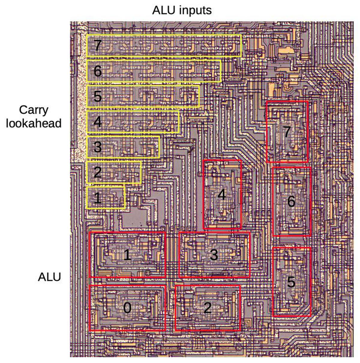
The diagram below zooms in on the carry lookahead circuitry and the arithmetic-logic unit (ALU). The two 8-bit arguments and a carry-in arrive at the top. These values flow vertically through the carry lookahead circuit, generating carry values for each bit along the way. Each ALU block receives two input bits and a carry bit and produces one output bit. The carry lookahead has a triangular layout because successive carry bits require more circuitry, as will be explained. The 8-bit ALU has an unusual layout in order to make the most of the triangular space. Almost all microprocessors arrange the ALU in a rectangular block; an 8-bit ALU would have 8 similar slices. But in the 8008, the slices of the ALU are scattered irregularly; some slices are even rotated sideways. I've written about the 8008's ALU before if you want more details.
To understand how carry lookahead works, consider three addition cases. First, adding 0+0 cannot generate a carry, even if there is a carry in; the sum is 0 (if there is no carry in) or 1 (with carry in). The second case is 0+1 or 1+0. In this case, there will be a carry out only if there is a carry in. (With no carry-in the result is 1, while with carry-in the result is 10.) This is the "propagate" case, since the carry-in is propagated to carry-out. The final case is 1+1. In this case, there will be a carry-out, regardless of the carry-in. This is the "generate" case, since a new carry is generated.
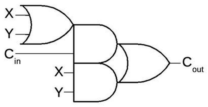
The circuit below computes the carry-out when adding two bits (X and Y) along with a carry-in. This circuit is built from an OR gate on the left, two AND gates in the middle, and an OR gate on the right. (Although this circuit looks complex, it can be implemented efficiently in hardware.) To see how it operates, consider the three cases. If X and Y are both 0, the carry output will be 0. Otherwise, the first OR gate will output 1. If carry-in is 1, the upper AND gate will output 1 and the carry-out will be 1. (This is the propagate case.) Finally, if both X and Y are 1, the lower AND gate will output 1, and the carry-out will be 1. (This is the generate case.)
To compute the carry into a higher-order position, multiple instances of this circuit can be chained together. For instance, the circuit below computes the carry into bit position 2 (C2). The gate block on the left computes C1, the carry into bit position 1, from the carry-in (C0) and low-order bits X0 and Y0, as explained above. The gates on the right apply the same process to the next bits, generating the carry into position 2. For other bit positions, the same principle is used but with additional blocks of gates. For instance, the carry into position 7 is computed by a chain of seven blocks of gates. Since the circuit for each successive bit is one unit longer, the carry structure has the triangular structure seen on the die.
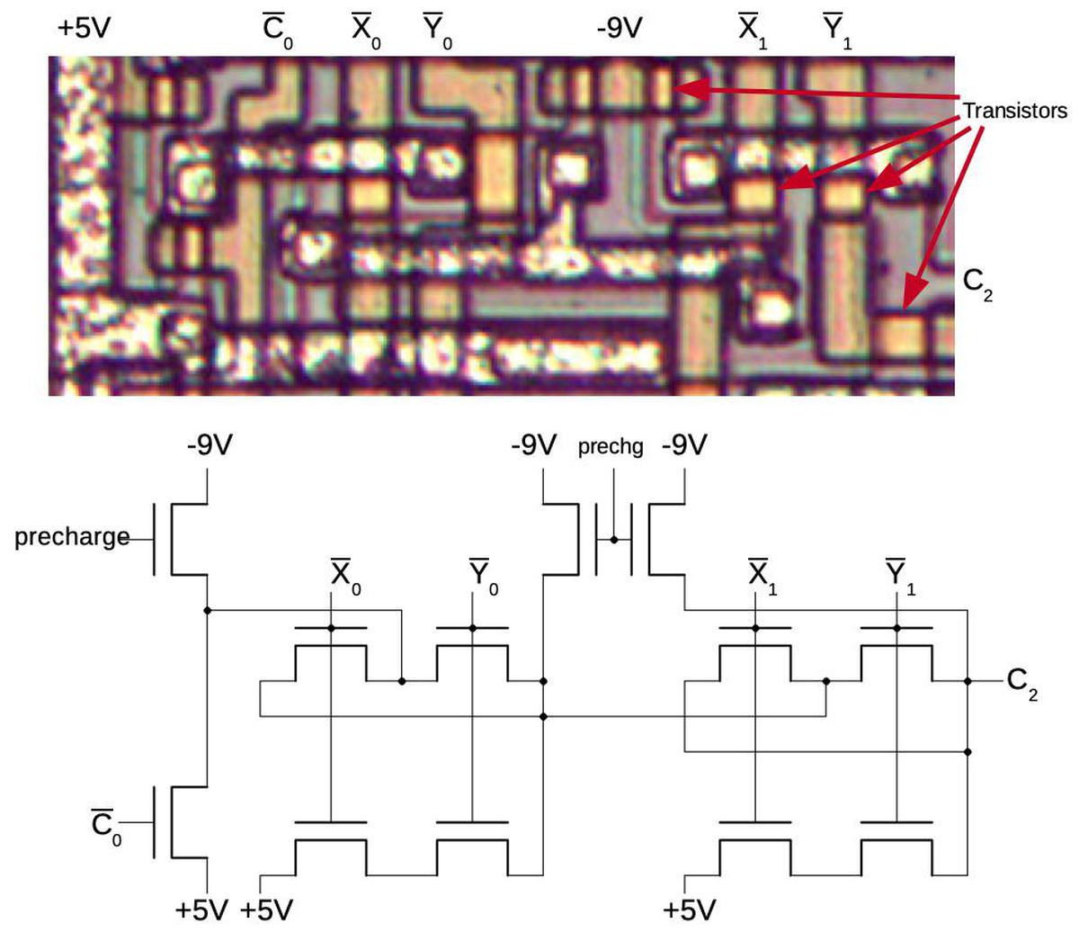
The diagram below shows how the carry circuit for bit 2 is implemented on the die; the circuit for other bits is similar, but with more repeated blocks. In the photograph, the metal wiring on top of the die is silverish. Underneath this, the polysilicon wiring is yellow. At the bottom, the silicon is grayish. The transistors are brighter yellow; several are indicated. The schematic underneath shows the wiring of the transistors; the layout of the schematic is close to the physical layout.
I'll give a brief outline of how the circuit works. The 8008 is implemented with a type of transistor called a PMOS transistor. You can think of a PMOS transistor as turning on if the input is 0, and off if the input is 1.4 Instead of standard logic gates, this circuit uses a technique called dynamic logic, which takes advantage of capacitance. In the first step, the precharge signal connects -9 volts to the circuitry, precharging it. In the second step, the input signals (top) are applied, turning on various transistors. If there is a path through the transistors from the +5 supply to the output, the output will be pulled high. Otherwise, the output remains at the precharge level; the capacitance of the wires holds the -9 volts. I won't trace out the entire circuit, but the upper X/Y transistor pairs implement an OR gate since if either one is on, the carry can get through. The lower X/Y transistors implement an AND gate; if both are on, the +5 signal will get through, generating a 1.
You might wonder why this carry lookahead circuit is any faster than a plain ripple-carry adder, since the carry signal has to go through up to seven large gates to generate the last carry bit. The trick is that the entire circuit is electrically a single large gate due to the dynamic design. All the transistors are activated in parallel, and then the 5-volt signal can pass through them all rapidly.5 Although there is still a delay as this signal travels through the circuit, the circuit is faster than the standard ripple carry adder which activates transistors in sequence.
A brief history of carry circuits
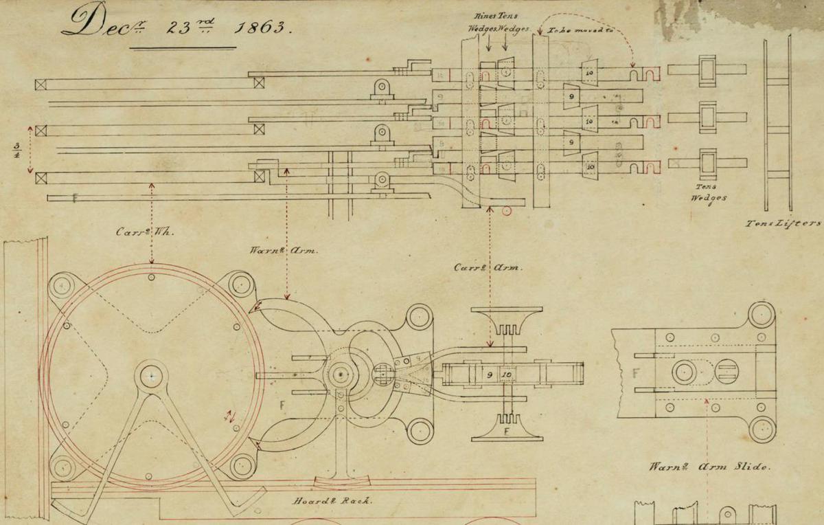
The efficient handling of carries was an issue back to the earliest days of mechanical calculation. The mathematician Blaise Pascal created a mechanical calculator in 1645. This calculator used a mechanical ripple carry mechanism powered by gravity that rapidly propagated the carry from one digit to the next (video). Almost two centuries later, Charles Babbage designed the famous difference engine (1819-1842). It used a slow ripple carry; after the addition cycle, spiral levers on a rotating shaft activated each digit's carry in sequence. Babbage spent years designing a better carry mechanism for his ambitious Analytical Engine (1837), developing an "anticipating carriage" to perform all carries in parallel. With the anticipating carriage, each digit wheel had a sliding shaft that moved into position when a digit was 9. When a digit triggered a carry by moving from 9 to 0, it raised the stack of shafts, incrementing all the appropriate digits in parallel (see video).
The first digital computers used ripple carry. The designer of the Bell Labs relay computer (1939) states that "the carry circuit was complicated" due to the use of binary-coded decimal (BCD). The groundbreaking ENIAC (1946) used decimal counters with ripple carry. Early binary electronic computers such as EDSAC (1949) and SEAC (1950) were serial, operating on one bit at a time, so they computed carries one bit at a time too. Early computers with parallel addition such as the 1950 SWAC (the fastest computer at the time) and the commercial IBM 701 (1952) used ripple carry.
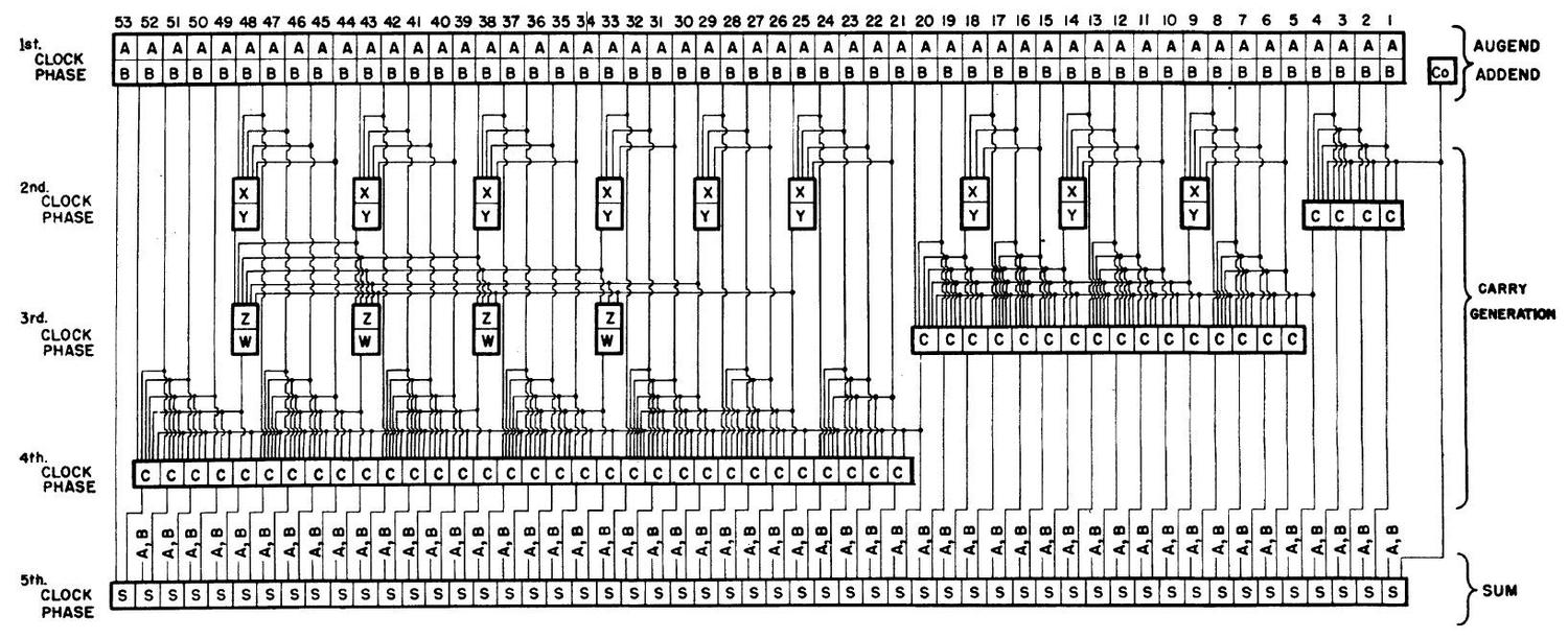
As computers became faster in the 1950s, ripple carry limited performance so alternatives were developed. In 1956, the National Bureau of Standards patented a 53-bit adder using vacuum tubes. This design introduced the important carry-lookahead concept, as well as the idea of using a hierarchy of carry lookahead (two levels in this case). The diagram below illustrates the complexity of this adder.
The development of supercomputers led to new carry techniques. The transistorized Atlas was built by the University of Manchester, Ferranti and Plessey in 1962. It used the influential Manchester carry chain technique, described in 1959. The Atlas vied with the IBM Stretch (1961) for the title of the world's fastest computer. The Stretch introduced high-speed techniques including the carry-select adder and the patented carry save adder for multiplication.
As with mainframes, microprocessors started with simple adders but required improved carry techniques as performance demands increased. Most early microprocessors used ripple carry, such as the 6502, Z-80, and ARM1. Carry-skip was often used for the program counter (as in the 6502 and Z-80); ripple carry was fast enough for 8-bit words but too slow for the 16-bit program counter. The ALU of the Intel 8086 (1978) used a Manchester carry chain as well as carry skip. The large transistor counts of VLSI chips permitted more complex adders, fed by research in parallel-prefix adders. The DEC Alpha 21064 (1992) combined multiple techniques: Manchester carry chain, carry lookahead, conditional sum, and carry select (details). The Hewlett-Packard PA_8000 (1995) contained over 20 adders for various purposes, including a Ling adder, a type developed at IBM in 1966 (details). The Pentium II (1997) used a 72-bit Kogge-Stone adder while the Pentium 4 (2000) used a Han-Carlson adder.6
This history shows that carry propagation was an important performance problem in the 1950s and remains an issue today with continuing research and improvements. Many different solutions have been developed, first in mainframes and later in microprocessors, growing more complex as technology advances. These approaches have tradeoffs of die area, cost, and speed, so different processors choose different implementations.
If you're interested in the 8008, I have other articles about it describing its architecture, its ALU, its on-chip stack, bootstrap loads, and its unusual history. I announce my latest blog posts on Twitter, so follow me at @kenshirriff. I also have an RSS feed.
Notes and references
-
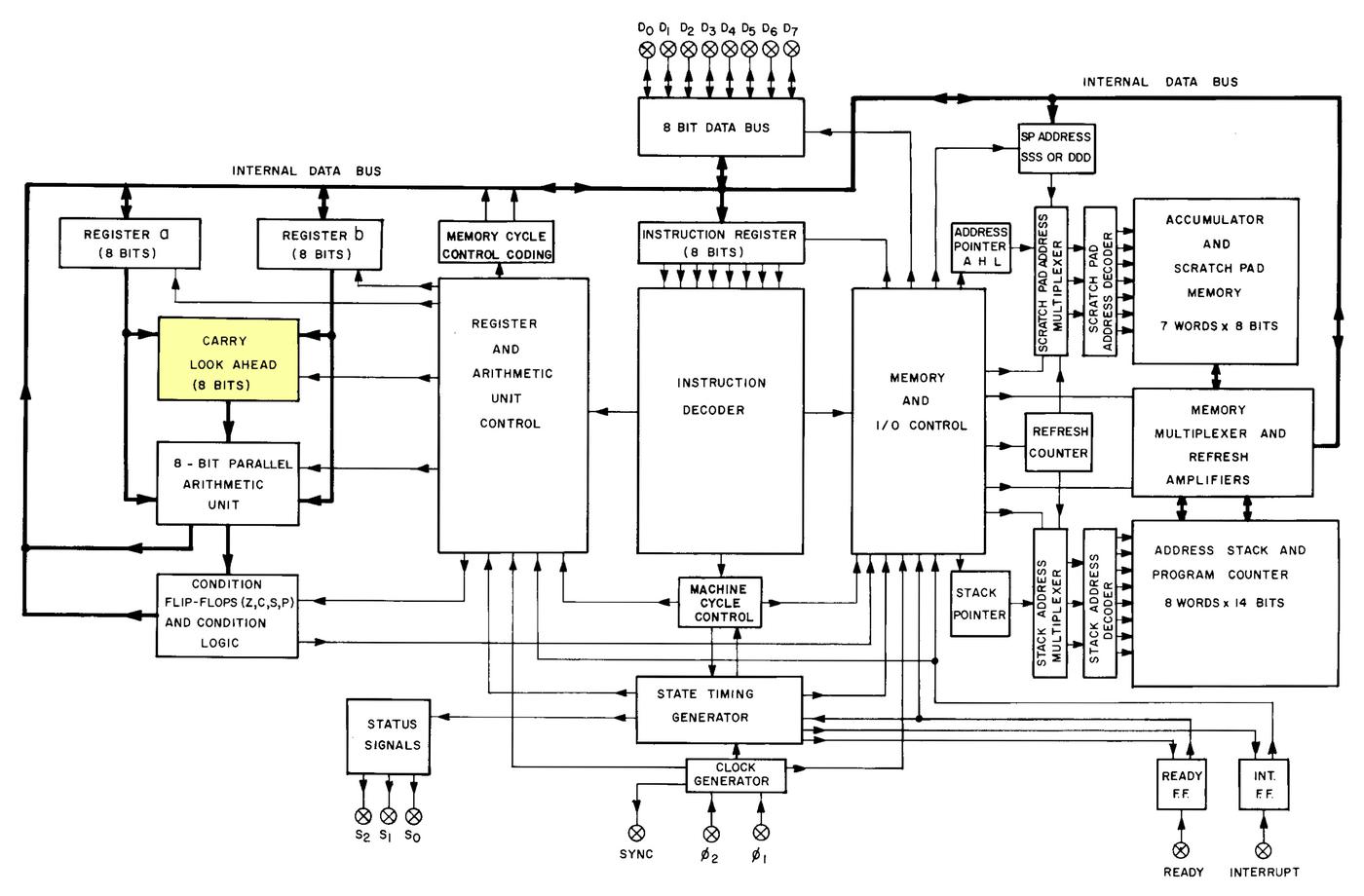
The functional blocks of the 8008 processor are documented in the datasheet (below). The layout of this diagram closely matches the physical layout on the die. I've highlighted the carry lookahead block.
Functional blocks of the 8008 processor. From the 8008 datasheet. -
According to Federico Faggin's oral history, the 8008 team was lucky to be allowed to even use an 18-pin package for the 8008. "It was a religion in Intel" to use 16-pin packages, even though other manufacturers commonly used 40- or 48-pin packages. When Intel was forced to move to 18-pin packages for the 1103 RAM chip, it "was like the sky had dropped from heaven. I never seen so [many] long faces at Intel". The move to 18 pins was beneficial for the 8008 team, which had been forced to use 16 pins for the earlier 4004. However, even 18 pins was impractically small considering the chip used 14-bit addresses. The result was address and data signals were multiplexed over 8 data pins. This both slowed the processor and made use of the chip more complicated. Intel soon gave up on small packages, using a standard 40-pin package for the 8080 processor in 1974. ↩
-
I'm ignoring subtraction in this discussion because it was implemented by addition, adding a two's complement value. Multiplication and division were not implemented by early microprocessors. Interestingly, even the earliest mainframe computers implemented multiplication and division in hardware. ↩
-
Most of the "classic" microprocessors were implemented with NMOS transistors. If you're familiar with NMOS gates, everything is backward with PMOS. Although PMOS has worse performance than NMOS, it was easier to manufacture at first, so the Intel 4004 and 8008 used PMOS. PMOS required fairly large negative voltages, which is why the diagram shows -9 volts and +5 volts. ↩
-
I'm hand-waving over the timing of the carry lookahead circuit. An accurate analysis of the timing would require considering the capacitance of each stage, which might add an O(n2) term.
Also note that this carry lookahead circuit is a bit unusual. A typical carry lookahead circuit (as in the 74181 ALU chip) expands out the gates, yielding much larger but flatter circuits to minimize propagation delays. On the other hand, the 8008's circuit has a lot in common with a Manchester carry chain, which uses a similar technique of passing the incoming carry through a chain of pass transistors, or potentially generating a carry at each stage. A Manchester carry chain, however, uses a single N-stage chain rather than the 8008's triangle of separate chains for each bit. A Manchester carry chain can tap each bit's carry from each stage of the chain, so only one chain is required. The 8008's carry circuit, however, lacks the transistors that block a carry from propagating backwards, so its intermediate values may not be valid.
In any case, the 8008's carry lookahead circuit was sufficiently fast for Intel's needs. ↩
-
For more information on various adders, see this presentation, another presentation and Advanced Arithmetic Techniques. ↩

Am I crazy, or could you add really fast with just a ROM. I guess you'd need a 17 bit address (8 bits for the 2 operands and 1 for carry) and you'd need 9 data bits to have the carry out, but it would be almost instantaneous in comparison, right? I guess it would be just too much real-estate, but maybe it could live outside the processor like a math coprocessor did. Of course then you have the overhead of passing it in and out which probably negates any adding speed. Not to mention it's 128K of 9 bit words which is kind of a lot of memory at that time. but you could split the problem into 2, 4-bit adds and just double the cycles. Did anybody ever try this for maximum adding speed or were these other techniques good enough. I guess making adding much faster wouldn't solve any problem if the rest of the chip couldn't keep up anyhow.
ReplyDeleteJosh O, I don't think there was ever a time when a >1Mbit ROM and an 8-bit ALU were ever economically viable in the same machine. In early days, or a low-cost machine, the ROM would have been too expensive, and in later days, or a high-end machine, an 8-bit ALU (even one built from a fast LUT ROM) would have been pitiful.
ReplyDeleteJosh, that's an interesting question. I'm not convinced that a ROM would be faster since the address has to go through a bunch of gates to be decoded. The long signal lines in the ROM have a lot of capacitance, which will slow you down. I looked at the vintage 2716 EPROM, and it takes 450 ns for access which is fairly slow. So a ROM isn't going to be an instantaneous silver bullet.
ReplyDeleteI should point out the low-end IBM 1620 scientific computer (1959), which used lookup tables for addition and subtraction, so your idea has been used in the past. This computer had the codename CADET. People joked that it stood for "Can't Add, Doesn't Even Try". The decimal lookup table in core memory was used as a cost-saving measure, not for performance.
In the company I worked in the 90s we did something in that vein. Of course not for a simple operation like add but for a complex wave form we needed for a special communication protocol. The protocol used a very specific waveform as carrier for the information and the chip to generate existed only from Phillips, it was extremely expensive and always on allocation. We managed to get away with a big fast eprom in which we stored the samples of the wave form, adding a bit of analogue circuitry to adapt the signal and voilà, cheaper card.
ReplyDeleteRobert Baruch did exactly this on his ALU board in his yet-unfinished LMARV-1 (Tangible RISC-V) processor. He explains carry propagate and generate in great detail, then goes on how to implement it (and all other ALU functions) with RAM chips as lookup tables.
ReplyDeletehttps://www.youtube.com/watch?v=KGBUtKRBKZs
Hi,
ReplyDeletethank you for another fascinating write-up.
This has been especially interesting to me because the chip is somewhat close to my heart. It had powered the first electronic toy I owned and I have written a crappy emulator in JaveScript for it this spring.
Amongst other things it includes a disassembler for the code the machine runs, a display of all 128 bytes of RAM and even breakpoints should you care about stopping the thing.
If you are interested you can find it at https://marian-aldenhoevel.de/jmerlin/.
very nice information
ReplyDeleteMy undergrad degree is Electronics Engineering (BSEL, 1973) from California Polytechnic State University, San Luis Obispo, CA. My senior year project was the first one at Cal Poly to use a microprocessor. Micros were expensive in those days. The 8008 listed for $300 each. I begged a cosmetic reject from Intel and they were gracious enough to provide one in a ceramic side brazed cavity package. The 8008 by itself didn't do anything but consume power. It required a halo of ~50 parts to function, and that was before you added memory. The project, a smart voltage gain calculating DVM, garnered a lot of attention from the faculty whose reaction ranged from "terrific project!" to "that thing is inadequate...". On the other hand, my two quarter project stretched to four quarters and became the pacing item to graduating on time. In retrospect I should have picked a less ambitious project, but that realization was part of the learning I came away with.
ReplyDeleteThere is a typo about the Analytical Engine: it was from 1837 (not 1937).
ReplyDeletevery well written and good information.
ReplyDeletehttps://abcofentertainment.com/2023/03/oscar-2023-nominations-and-winners/