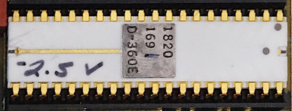
In 1974, Hewlett-Packard developed a microprocessor for control applications in their products, from floppy disk drives to voltmeters. This simple processor was a step down from the typical microprocessor—it didn't even support addition or subtraction1—so it was called the Nanoprocessor. The Nanoprocessor's key features were its low cost and high speed: compared against the contemporary Motorola 6800, the Nanoprocessor cost $15 instead of $360 and performed control tasks an order of magnitude faster.
This processor remained obscure for decades until its designer, Larry Bower, recently donated the chip's masks and documentation to The CPU Shack, who scanned the masks and wrote about the Nanoprocessor. After Antoine Bercovici stitched together the images,2 I wrote a Nanoprocessor overview article based on them. This blog post is part two, where I discuss some of the Nanoprocessor circuitry in detail, reverse-engineering it from the masks. These functional blocks are interesting to study because the Nanoprocessor strips its implementation down to the minimum, while still remaining a useful microprocessor.
Inside the Nanoprocessor
Like most processors of that era, the Nanoprocessor was an 8-bit processor. However, it didn't support RAM,3 but ran code from an external 2-kilobyte ROM. It contained 16 8-bit registers, more than most processors and enough to make up for the lack of RAM in many applications. The Nanoprocessor had 48 instructions, a considerably smaller instruction set than the Motorola 6800's 72 instructions. However, the Nanoprocessor included convenient bit set, clear, and test operations, which other processors of that era lacked. It also had multiple I/O instructions supporting both I/O ports and general-purpose I/O pins, making it easy to control devices with the Nanoprocessor.
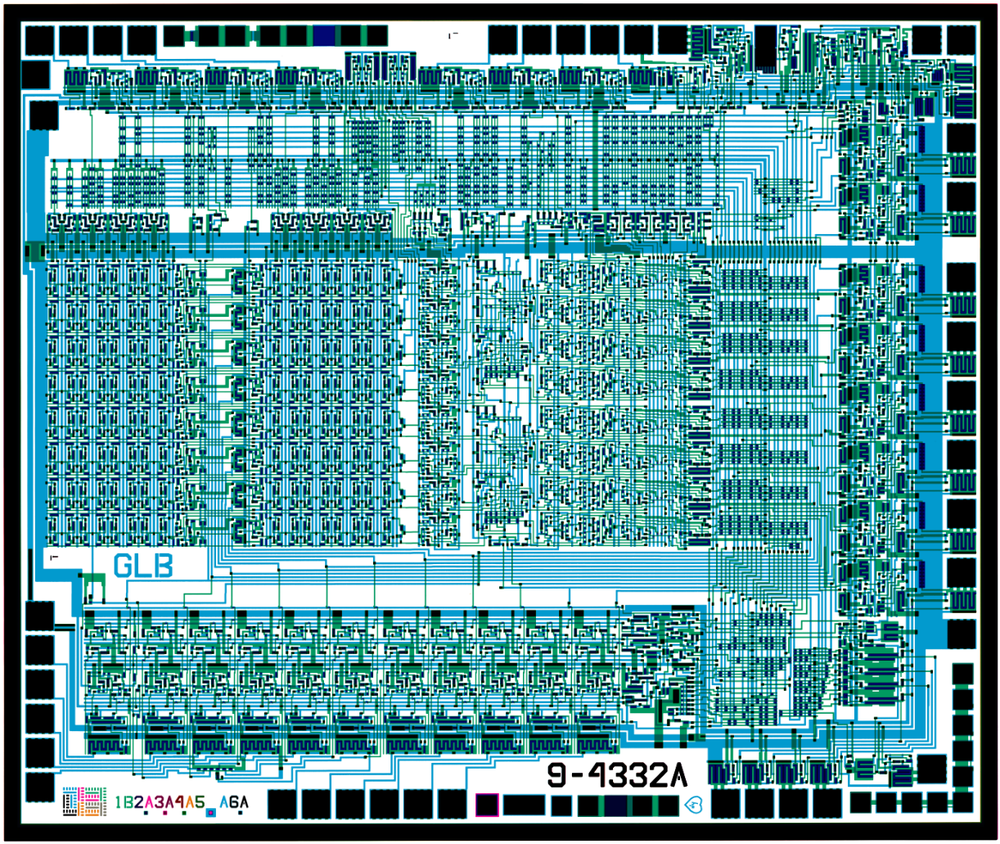
The mask image above shows the simplicity of the Nanoprocessor. The blue lines show the metal wiring on top of the chip, while the green shows the doped silicon underneath. The black squares around the outside are the 40 pads for connection to the IC's external pins. The small black regions inside the chip are transistors; if you squint, you should be able to count 4639 of them.4
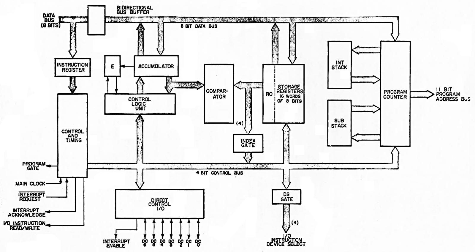
The block diagram below shows the internal structure of the Nanoprocessor. The 16 storage registers are in the middle. The comparator allows two values to be compared for conditional branches. The Control Logic Unit performs increments, decrements, shifts, and bit operations on the accumulator, lacking the arithmetic and logical operations of a standard Arithmetic/Logic Unit (ALU). The program counter (right) fetches an instruction into the instruction register (left); interrupts and subroutine calls each have a one-entry stack for the return address.
I should emphasize that despite its simplicity5 and lack of arithmetic, the Nanoprocessor is not a "toy" processor that just toggles some control lines, but a fast and capable processor used for complex tasks. The HP 98035 real-time clock module, for instance, uses the Nanoprocessor to parse two dozen different ASCII command strings, as well as activities such as calculating the number of days in each month.
Registers
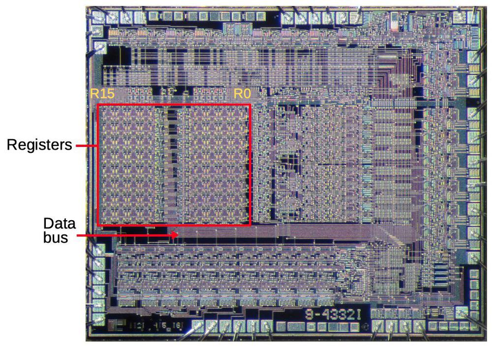
The die photo below shows that much of the Nanoprocessor's die is occupied by its 16 registers. These registers communicate with the rest of the chip via the data bus. Circuitry above the registers selects a particular register. Register R0, on the right, is next to the comparator, which will be important later.
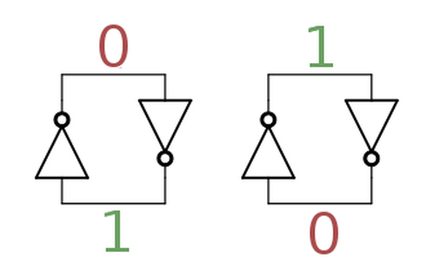
The building block for the registers is two inverters in a feedback loop, storing a single bit as shown below. If the top wire has a 0, the right inverter will output a 1 to the bottom wire. The left inverter will then output a 0 to the top wire, completing the cycle. Thus, the circuit is stable and will "remember" the 0. Likewise, if the top wire is a 1, this will get inverted to a 0 at the bottom wire, and back to a 1 at the top. Thus, this circuit can store either a 0 or a 1, forming a 1-bit memory.
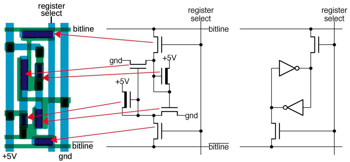
The diagram below shows how this two-inverter storage is implemented on the die. The left shows the physical layout, from the mask images. The layout is optimized to make the cell as small as possible. Blue lines indicate the metal layer, while green is the silicon layer. The schematic in the middle shows the corresponding transistor circuitry. Each inverter is formed from a pair of transistors, as shown on the right. The top and bottom transistors are "pass transistors", providing access to the storage cell.
The register set is built from a matrix of these bit cells. The register select line selects one register (one column) for reading or writing. When selected, the top and bottom pass transistors connect the inverters to the corresponding horizontal bitlines. For a read operation, the top bitline provides the value stored in the cell; there are eight pairs of bitlines for the eight bits in a register. For a write operation, the value is applied to the upper bitline and the inverted value is applied to the lower bitline. These values overpower the signals from the inverters, forcing the inverters to the desired value and storing the bit. Thus, the grid of horizontal bitlines and vertical select lines allows a particular register to be read or written.
Instruction decoding
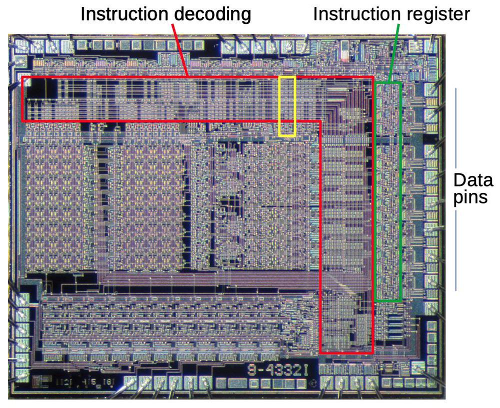
The instruction decoding circuitry is responsible for taking a binary instruction code (such as 01101010) and determining what instruction it is ("Load accumulator from register 10" in this case). Compared to many processors, the Nanoprocessor's instructions are pretty simple: it has relatively few instructions (48) and the opcode is always one byte long. The diagram below shows that instruction decoding logic (red) takes up a large fraction of the chip. The instruction register (green), is a set of eight latches holding the current instruction. The instruction register is next to the data pins, which provide the instruction from the ROM. This section will focus on the decoding circuit in the yellow box.
Decoding is done by NOR gates; each NOR gate detects a particular instruction or group of instructions.
The NOR gates take instruction bits or their complements as inputs. When all inputs are zero, the NOR gate indicates
a match.
This allows matching against the entire instruction or part of the instruction. For instance, the "Load accumulator from register R" instruction has the binary format "0110rrrr", where the last four bits indicate the desired register.
A NOR gate (bit7 + bit6' + bit5' + bit4)' will match instructions of that form.
The nice thing about structuring the instruction decoder in this way is that it can be built from compact, regular circuits, often called a PLA.6 The idea is to make a matrix with input signals running horizontally and outputs vertically. Each intersection can have a transistor, making the input signal part of the gate; or no transistor, ignoring that input signal. The result is tightly-packed NOR gates.
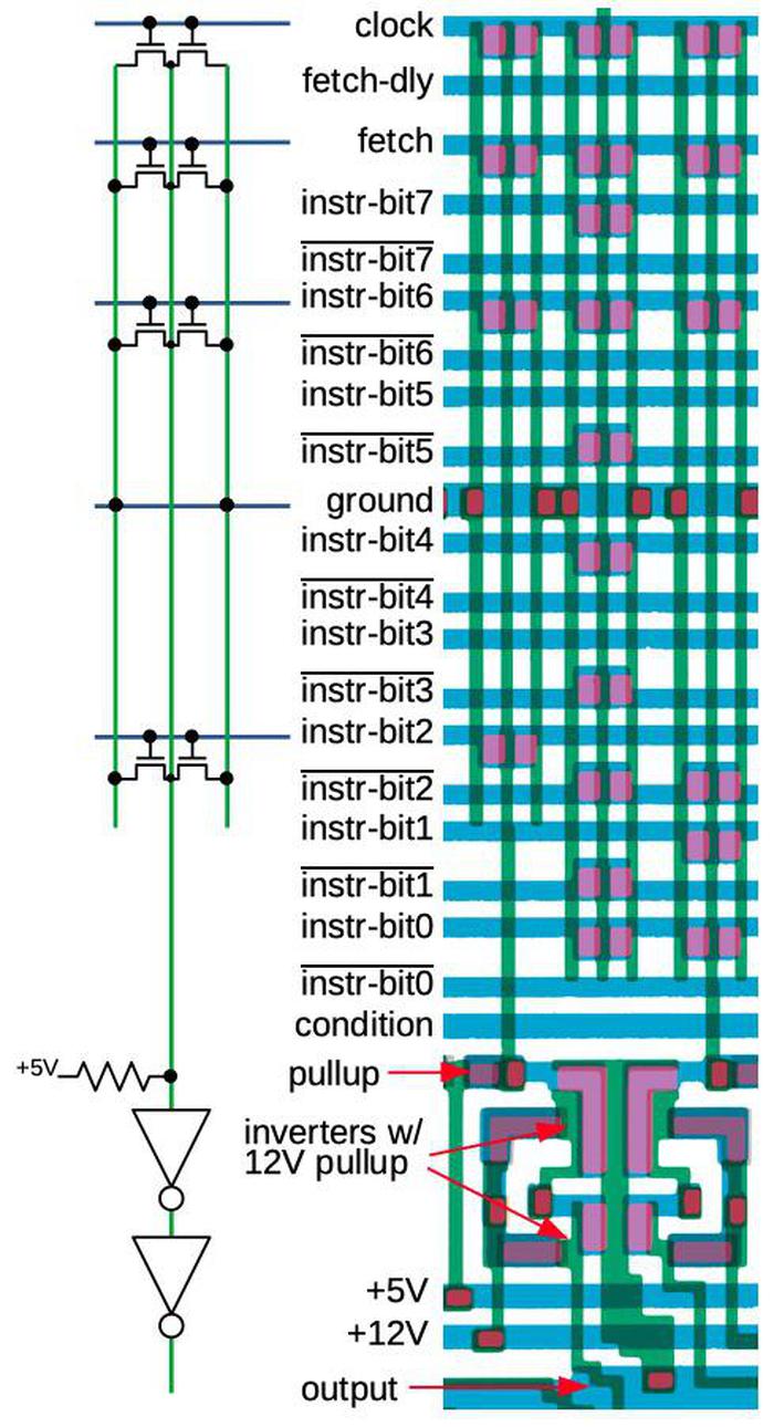
The diagram on the right below zooms in on the three decoders highlighted in yellow above. The schematic corresponds to the leftmost decoder; note the correspondence between transistors in the schematic and the pink transistor blobs in the layout. The idea is that if any input energizes a transistor, the transistor will pull the output to ground. Otherwise, the output is pulled high by the resistor. The inverters at the bottom amplify the signal, providing enough current to drive all eight slices of the accumulator.7 Curiously, the layout uses pairs of transistors, both connected between ground and the output; I don't see the advantage over the straightforward approach of using a single transistor. In any case, note how the PLA-style matrix provides a dense layout for the decoders.
This particular circuit generates the increment/decrement signal that is fed into the accumulator circuit. This circuit matches when the clock, fetch, instruction bit 6, and instruction bit 2 are all low, so it matches instructions of the form x0xxx0xx during execute phase. These instructions include "Increment Binary" (00000000), "Increment BCD" (00000010), "Decrement Binary" (00000001) and "Decrement BCD" (00000011).8
Comparator
An important circuit in the Nanoprocessor is the comparator that determines if the accumulator A is greater, less than, or equal to register R0. The comparator uses a simple but clever circuit to compare these two values. The algorithm is essentially to compare the two numbers starting with the most significant bits. As long as the bits are equal, keep moving to the less significant bits. The first difference between the two numbers determines which one is greater. (For instance, with 10101010 and 10100111, the highlighted bits determine that the first number is greater.)
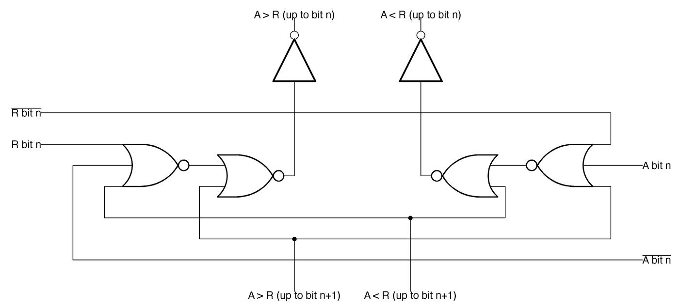
This algorithm is implemented with eight stages, one for each bit, starting with the most significant bits at the bottom. Each stage (below) consists of two symmetrical parts: one determines if A > R0, while the complementary one determines if A < R0. If the numbers are equal so far, but the two bits are different at this stage, the stage generates the greater than or less than signal. Otherwise, it passes along the decision of the lower stage. The topmost stage outputs the final decision. Note that the comparator provides an equality test "for free"; if the output isn't greater than or less than, the two numbers are equal.
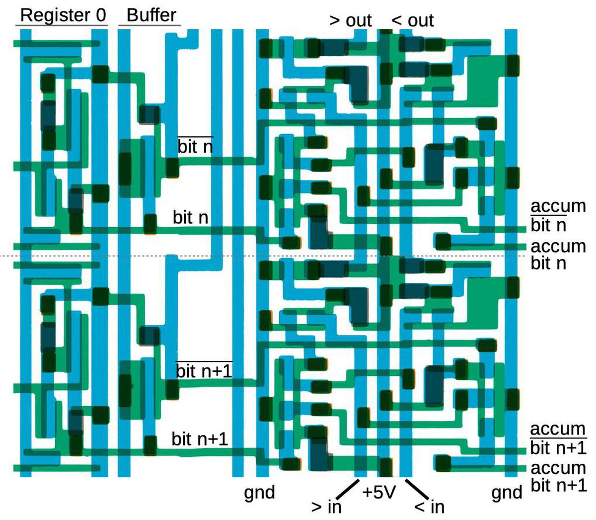
The diagram below shows the physical layout of two comparator stages. One clever feature of the comparator's layout is that it sits between register 0 on the left and the accumulator on the right, minimizing wiring. The comparator accesses register 0 directly, without going through the regular path of the register selection and the data bus.
The Nanoprocessor's conditional branch instructions can test the comparator outputs.9 The branch circuitry is fairly straightforward: several bits of the branch instruction select the particular test via a multiplexer. Then bit 7 of the instruction selects "branch if true" versus "branch if false". Unlike most processors, the Nanoprocessor doesn't provide branches to an arbitrary address. Instead, it skips two instruction bytes if the condition is satisfied. (Typically these two bytes would hold a jump to the desired target, but sometimes hold other instructions.) The skip circuit is simple: the program counter incrementer (described below) is triggered a second time, but increments by two instead of one, skipping two instructions. Thus, the Nanoprocessor implements an extensive set of conditional tests with a relatively small amount of circuitry.
Accumulator and Control Logic Unit
The accumulator is the special 8-bit register that stores the byte currently being processed. Operations on the accumulator are performed by the Control Logic Unit (CLU), which the manual calls "the heart of the Nanoprocessor". The CLU is the equivalent of the Arithmetic/Logic Unit (ALU) in most processors, except it doesn't perform arithmetic or logic operations. The CLU is not quite as useless as it sounds, though. It can increment or decrement the accumulator, both in binary and binary coded decimal (BCD). (Binary coded decimal stores two decimal digits per byte. This is very useful for decimal I/O or displays.) The CLU can also complement or clear the accumulator, or set or clear a specific bit. Finally, it supports left and right shift operations.
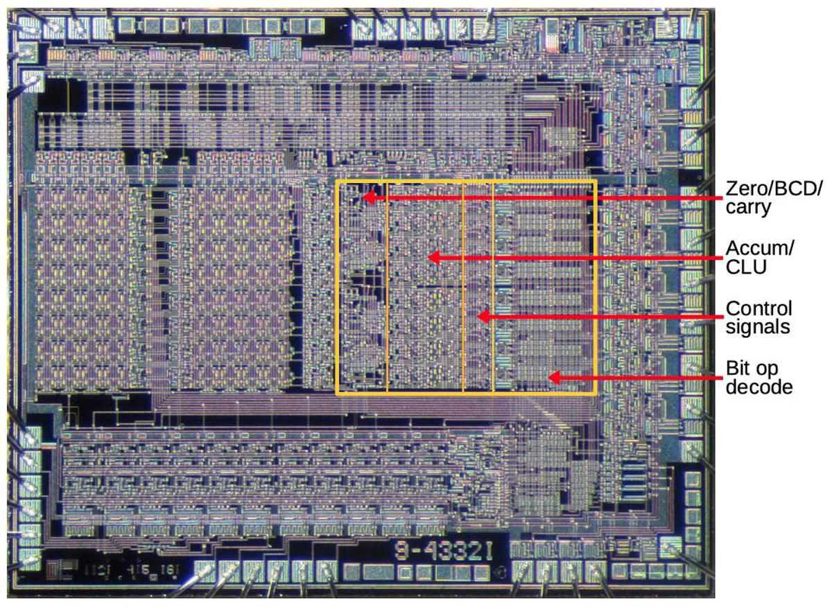
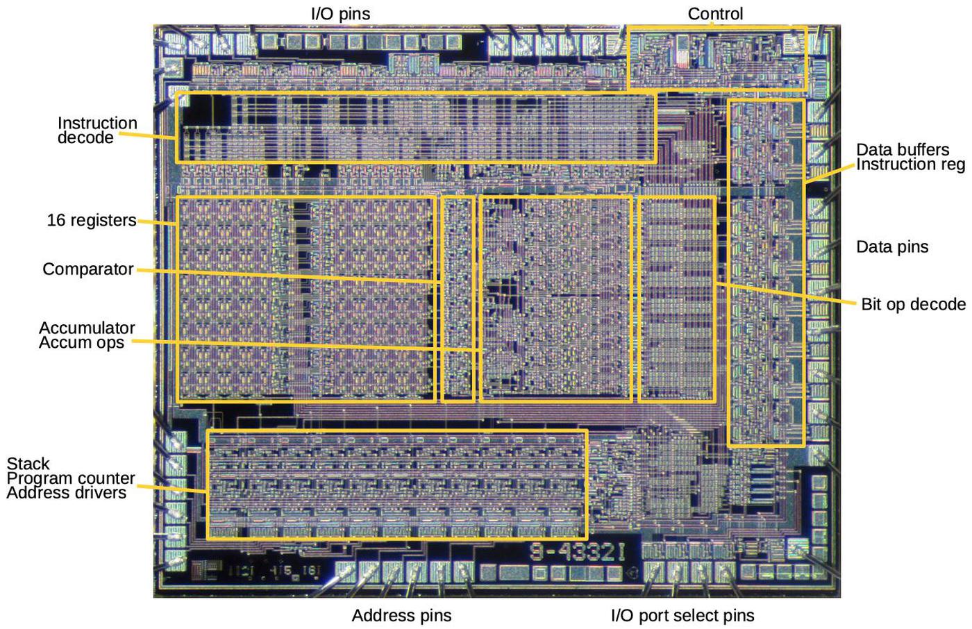
The diagram above shows the layout of the accumulator and CLU. The first region has miscellaneous circuitry to detect a zero value; support BCD by detecting a 9 digit, for instance; and provide carry-skip, fast carry generation from the lower 4 bits. I won't discuss this in more detail, but note the irregular layout of this circuitry. The second region holds the main accumulator and CLU circuitry; I will discuss this in detail below. The third region distributes control signals from the decode logic above to the eight accumulator slices. Finally, the last region holds instruction decoding logic to decode bit operations and signal the appropriate accumulator slice.
The main part of the accumulator/CLU consists of 8 slices, one for each bit, with the lowest bit at the top. I will discuss four circuits in each slice: the incrementer/decrementer's carry generation, the incrementer/decrementer's bit generation, the multiplexer to select the new accumulator value, and the latch that holds the accumulator's value.
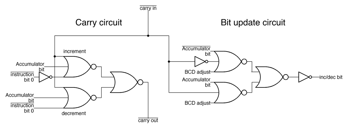
Each slice of the incrementer/decrementer (below) is implemented by a half adder. The direction of the incrementer/decrementer circuit depends on the opcode: a 0 in the opcode's low bit indicates an increment, while a 1 in the opcode's low bit indicates a decrement. The carry circuit on the left below generates the carry-out signal. For an increment, there is a carry-out if there is a carry-in and the current bit is 1 (since it will be incremented to binary 10). For decrement, the carry line indicates a borrow, rather than a carry, so there is a carry-out if there is a carry-in (i.e. a borrow) and the current bit is 0, triggering a borrow.
The circuit on the right above updates the current bit when incrementing or decrementing. The current bit is flipped if there is a carry-in, essentially an XOR implemented by three NOR gates. One complication is the adjustment for BCD (binary-coded decimal). For a BCD increment operation, a carry occurs when incrementing a 9 digit, while for a BCD decrement, a 0 digit is decremented to 9, not to binary 1111.
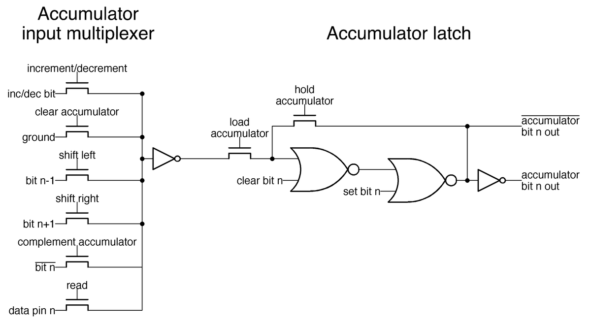
The different accumulator operations are provided by the multiplexer below. Depending on the operation, one pass transistor will be activated, selecting the desired value. For instance, for an increment/decrement operation, the top transistor selects the output from the increment/decrement circuit described above. This transistor is activated by the instruction decoder described earlier that matches an increment/decrement instruction. Similarly, a shift-right instruction activates the shift-right pass transistor, feeding accumulator bit n+1 into each accumulator slice to shift the value.
The latch above stores one bit of the accumulator. When the hold accumulator transistor is activated, the two NOR gates form a loop, holding the value. But when the load accumulator transistor is activated instead, the accumulator loads its value from the multiplexer. The clear bit n and set bit n lines allow instructions to modify individual bits of the accumulator; the multiplexer, in comparison, updates all accumulator bits at once.
Program counter and addressing
Another large block of circuitry is the 11-bit program counter in the lower left of the Nanoprocessor, which I'll describe briefly. This block also includes a latch to hold the return address for a subroutine call and a second latch to hold the program counter after an interrupt. (You can think of these as one-entry stacks.) The program counter includes an incrementer to advance it to the next instruction. This incrementer can also increment by two, allowing conditional branch instructions to skip over two instructions. (Increment-by-two is implemented by incrementing bit 1 instead of bit 0.) To improve the performance of the incrementer, it has a carry-skip feature; if the bottom six bits are all 1, it will increment bit 6 immediately without waiting for the carry to propagate through the low-order bits.
Control and timing
The final piece of the Nanoprocessor is the control circuitry. Compared to other microprocessors, the Nanoprocessor's control circuitry is almost trivial: the processor alternates between fetch and execute cycles (with the occasional interrupt). The control circuitry is not much more than a couple of flip flops and gates, so I won't say more about it.
Conclusions
The diagram below summarizes the main functional blocks of the Nanoprocessor. The Nanoprocessor achieves a dense layout for these blocks, much better than I would expect from its obsolete metal-gate technology.10 Reverse-engineering shows that these functional blocks are implemented with simple but carefully-designed circuits.
The Nanoprocessor is an unusual processor. My first impression was that it wasn't even a "real processor," since it lacked basic arithmetic functionality. However, after studying it, I'm more impressed. Its simple design allows it to operate faster than other processors of the time. The instruction set is more capable than it appears at first. Hewlett-Packard used the Nanoprocessor in many products in the 1970s and 1980s, in roles that were more complex than you'd expect, such as parsing strings and performing calculations. Now, with the masks released by The CPU Shack, we can learn the secrets of the circuits that made the Nanoprocessor work.
Follow me on Twitter at @kenshirriff for updates on my blog posts. I also have an RSS feed. Thanks to Antoine Bercovici for scanning and remastering the masks, Larry Bower for the donation, and John Culver at The CPU Shack for sharing the donation.
Notes and references
-
Although it lacks an addition instruction, the Nanoprocessor can add numbers (slowly) through repeated increment and decrement operations (which it supports). (The code for the HP real-time clock module does this.) Other applications, such as the HP voltmeter, added external ALU chips (74LS181) to perform fast addition; these were accessed as I/O devices. (With Turing-completeness, of course, the Nanoprocessor can theoretically do anything from floating-point functions to Crysis; it will just be very slow.) ↩
-
The mask images can be downloaded here (warning: 122 MB PSD file). ↩
-
The Nanoprocessor doesn't have instructions to support RAM, since it is designed for control applications that typically don't need much storage. However, some Nanoprocessor applications use RAM, treating RAM as an I/O device. The address is written to one I/O port and the data byte is read or written from another port. ↩
-
By my count, the Nanoprocessor has 4639 transistors. The instruction decoder is constructed from pairs of small transistors for layout reasons; combining these pairs yields 3829 unique transistors. Of these, 1061 act as pull-ups, while 2668 are active. In comparison, the 6502 has 4237 transistors, of which 3218 are active. The 8008 has 3500 transistors and the Motorola 6800 has 4100 transistors. ↩
-
Making an FPGA version of the Nanoprocessor would probably be a fun project since the Nanoprocessor is about as simple as you can make a real, commercial processor. The User's Guide explains the instructions and has sample code that could be executed. ↩
-
Building the decoder out of an array of NOR gates decoding was common in early microprocessors, for instance the 6502, because it could be constructed in a regular, compact form. It's often called a PLA (Programmable Logic Array), even though a PLA is supposed to have two layers of logic. ↩
-
Note that the inverters in the instruction decoder are pulled up to 12 volts, rather than 5 volts. The reason is that the Nanoprocessor uses metal-gate transistors, rather than the more advanced silicon-gate transistors of other microprocessors of the era. Metal-gate transistors have the disadvantage of a higher threshold voltage, which means the output of a transistor is considerably lower than the gate voltage. The output from a regular inverter is too low to drive the gate of a pass transistor, since the output will be another threshold voltage below that. The solution is to use the 12 volt supply for the decoder inverters that drive pass transistors in the accumulator. Then, these signals have plenty of voltage to drive pass transistors. In other words, the Nanoprocessor required an extra +12V supply because it used metal-gate transistors instead of the more modern silicon-gate transistors. ↩
-
The illustrated decode circuit matches against instructions x0xxx0xx, so it matches against many more instructions than just the increment and decrement instructions. Why doesn't the circuit match exactly? The reason is that if the accumulator is not being used, it doesn't matter if the increment/decrement signal is activated. By making the match wider, the designers could omit some transistors. The important point is that the circuit rejects other accumulator instructions such as "Clear accumulator" (00000100) or "Load accumulator from register" (0110rrrr). ↩
-
The Nanoprocessor has an extensive set of conditional branches, surprisingly many for a simple processor. You can branch if A > R0, A >= R0, A < R0, A <= R0, A == R0, or A != R0. In additional conditional branches can be done on the accumulator being zero or nonzero, any particular bit of the accumulator being zero or nonzero, the overflow flag being set or not, or a particular general-purpose I/O ("direct control") bit being set or not. ↩
-
The Nanoprocessor used metal-gate transistors, while other microprocessors started using silicon-gate transistors a few years earlier. This may seem like an obscure difference, but it has a huge impact on layout: silicon-gate fabrication added a layer of polysilicon wiring. This makes layout much easier, since you now have two layers for wiring that can cross each other. With just the metal layer for wiring, like the Nanoprocessor, layout is difficult because wires keep getting in the way of each other. In other metal-gate chips that I've examined, the layout is just awful; there's a lot of convoluted wiring to get the signals to each transistor, so the transistor density is low. In comparison, the Nanoprocessor's functional blocks are all carefully designed so the signals all flow together nicely. There's some wasted space, for instance for the data bus, but overall, I'm impressed by the density of the Nanoprocessor's layout. ↩
My limited experience with microcontrollers is that cost and function are the primary goals, performance isn't as important.
ReplyDeleteIt seems that HP used this chip to bang bits a lot more than add numbers, so that makes sense. I wonder why at some point later on, they didn't follow on with another design with a more complete ALU?
"The blue lines show the metal wiring on top of the chip, while the green shows the silicon underneath"
ReplyDeleteIt might be a little clearer to say that "the green shows the doped silicon underneath" since there is silicon everywhere in the chip. Even that is a simplification, since the bulk silicon is also doped but more lightly and in the opposite polarity of the green areas.
Jecel: good point; I updated the text.
ReplyDeletePerfect timing for this article: I was starting practicing some chip RE basing on your first one on nanoprocessor.
ReplyDeleteMay I ask for your interpretation of a couple of mysterious (to me) objects on the chip, please?
The first is in the clock/control circuitry, at coordinates (8500,500) in the PSD file. It looks like a pad but it's not. Could that be a kind of capacitor to time the reset pulse? The NP has no external reset signal and it must generate it internally when supply voltages rise.
There are other funny looking objects that are only used for D7-D0 lines, one is at (10250,1560).
My guess is that they are some kind of protection diode.
Thanks for your hints.
F.Ulivi: yes, I believe the pad-like thing is a large capacitor. The Nanoprocessor requires the Vgg power pin to go high a bit after the other power supplies. This causes the internal reset signal to be generated, and the capacitor provides the delay as you suggested. This approach avoids using a separate pin for reset, but makes the power supply design more complex.
ReplyDeleteI'm not entirely about the structures on the input pins. My guess is current-limiting resistors.
I don't understand how the PLA works. Isn't a single transistor enough to pull the output low? If so, where does the AND function come from? Is the pull up resistor sized such that it takes N transistors to overpower it? But I cannot see how you can get a reliable high voltage with 9 transistors and a reliable low with 10 transistors (assuming the worst case of matching b11111111 with CLOCK and FETCH).
ReplyDelete