The Intel 8086 microprocessor is one of the most influential chips ever created; it led to the x86 architecture that dominates desktop and server computing today. But it is still simple enough that its circuitry can be studied under the microscope and understood. In this post, I explain the implementation of a dynamic latch, a circuit that holds a single bit. The 8086 has over 80 latches scattered throughout the chip, holding a variety of important processor state bits,1 but I'll focus on the eight latches that implement the instruction register and hold the instruction that is being executed.
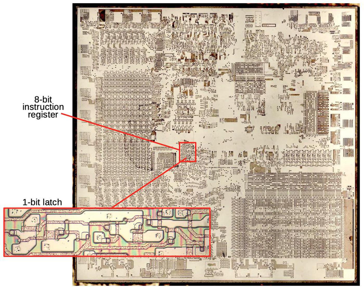
The photo above shows the silicon die of the 8086 processor under a microscope. I removed the metal and polysilicon layers to reveal the transistors, approximately 29,000 of them. The highlighted region indicates the 8086's 8-bit instruction buffer, consisting of eight latches. (This 1978 processor is simple enough that a single 8-bit register occupies a substantial region of the die.) The closeup shows the silicon and transistors making up a single latch.
The dynamic latch and how it works
The latch is one of the most important circuits in the 8086, since the latches keep track of what the processor is doing. While latches can be made in many ways,2 the 8086 uses a compact circuit called the dynamic latch. The dynamic latch depends on a two-phase clock, commonly used to control microprocessors of that era.3 A two-phase clock consists of two clock signals that are active in alternation. In the first phase, clock is high and the complement clock is low. Then they switch so clock is low and clock is high. This cycle repeats at the clock frequency, such as 5 MHz.
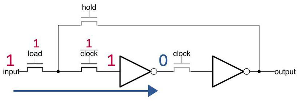
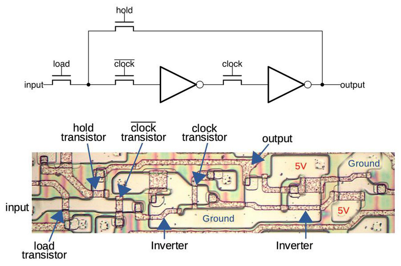
The schematic above shows a typical latch in the 8086. It consists of two inverters and several pass transistors. For our purposes, the pass transistor can be considered a switch: if the gate input is 1, the transistor passes the signal through. If the gate input is 0, the transistor blocks the signal. The pass transistors are controlled by several signals: load, which loads a bit into the latch; hold, which holds the existing bit value; clock, the first clock phase; and clock, the second, inverted clock phase.
The diagram below shows how a value (1 in this case) is loaded into the latch. The load signal is brought high, allowing the input (1 in this example) to pass through the first transistor. Since clock is high, the signal passes through the second transistor to the inverter, which outputs 0. At this point, the third (clock) transistor blocks the signal.
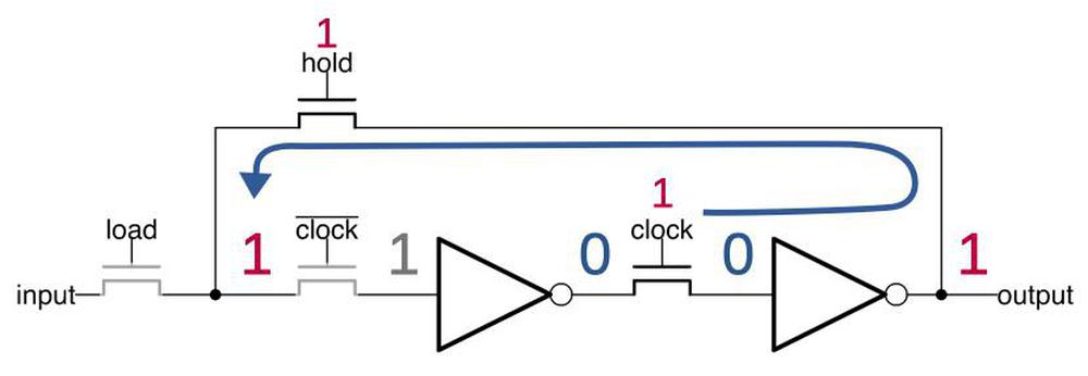
In the next clock phase (below), clock goes high, allowing the 0 signal to reach the second inverter, which outputs 1. Since hold is high, the signal loops back, but is blocked by the clock transistor. The important point, which makes this circuit dynamic, is that at this time there is no active input to the first inverter. Instead, its input remains 1 (shown in gray) due to the capacitance of the circuit. Eventually, this charge would leak away, losing the value, but before that happens, the clocks toggle.
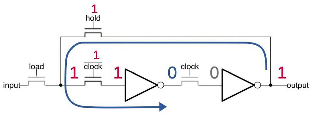
After the clocks switch state, the second inverter's input is provided by the capacitance of the circuit (below). The signal loops around, recharging and refreshing the input to the first inverter. As the clock signals continue to toggle, the latch switches between this diagram and the previous diagram, preserving the value in the latch and keeping the output stable.4
The implementation in silicon
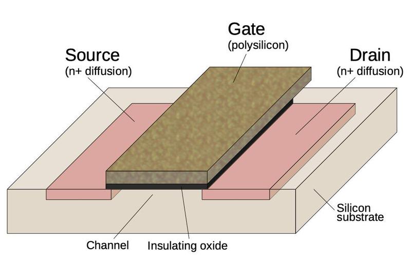
The 8086 and other processors of that era were built from a type of transistor called NMOS. They were constructed from a silicon substrate that was "doped" by diffusion of arsenic or boron to form the transistors. On top of the silicon, polysilicon wiring created the gates of the transistors and wired components together. Finally, a metal layer on top provided more wiring. (In comparison, modern processors are built from CMOS technology, which combines NMOS and PMOS transistors, and they have many layers of metal wiring.)
The diagram above shows the structure of a transistor. The transistor can be viewed as a switch, allowing current to flow between two diffusion regions called the source and drain. The transistor is controlled by the gate, made of a special type of silicon called polysilicon. Applying voltage to the gate lets current flow between the source and drain, while pulling the gate to 0 volts blocks the current flow. The gate is separated from the silicon by an insulating oxide layer; this makes the gate act like a capacitor as seen in the dynamic latch.
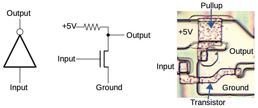
An inverter (below) is built from an NMOS transistor and a resistor.5 With a low input, the transistor is off, so the pull-up resistor pulls the output high. With a high input, the transistor turns on. This connects the output to ground, pulling the output low. Thus, the circuit inverts the input signal.
The photo on the right shows how an inverter is physically constructed in the 8086. The yellowish regions are conductive doped silicon and the speckled regions are the polysilicon on top. A transistor is created where polysilicon crosses doped silicon: the polysilicon forms the transistor's gate, while the silicon regions on either side are the transistor's source and drain. The large polysilicon rectangle forms the pull-up resistor between +5 volts and the output. These physical structures can be matched with the schematic.
The diagram below shows the implementation of a latch on the chip. The pass transistors and the two inverters are indicated; the first inverter is the one described above. Polysilicon wiring connects the components together; the metal layer (removed) provided additional wiring. The transistors have complex shapes to make the most efficient use of the space.
The latch includes output buffers, not shown on the schematic above, that provide high-current signals for the output and inverted output. This type of buffer has the amusing name "superbuffer" because it provides much higher current than a regular NMOS inverter. The problem with an NMOS inverter is it is slow when driving something with high capacitance. Since the superbuffer provides more current, it will switch the signal much faster. The superbuffer accomplishes this by replacing the pullup resistor with a transistor, which provides higher current. The downside is that the pullup transistor requires an inverter to drive it, so the superbuffer circuit is more complex. Thus, superbuffers are only used when necessary, typically when sending a signal to many gates or when driving a long bus line.
The diagram above shows the superbuffer circuit in the 8086's latches. Unlike the typical superbuffer, this one includes both an inverting and non-inverting superbuffer. To understand the circuit, note that the central resistor and transistor form an inverter. The inverter output is connected to the upper transistors, while the uninverted input is connected to the lower transistors. Thus, if the input is 1, the lower transistors will turn on, while if the input is 0, the upper transistors will turn on due to the inverter. Thus, for a 1 input, the lower transistors will pull Output high and the complement Output low. But for a 0 input, the upper transistors will pull Output low and the complement Output high.6
The instruction register
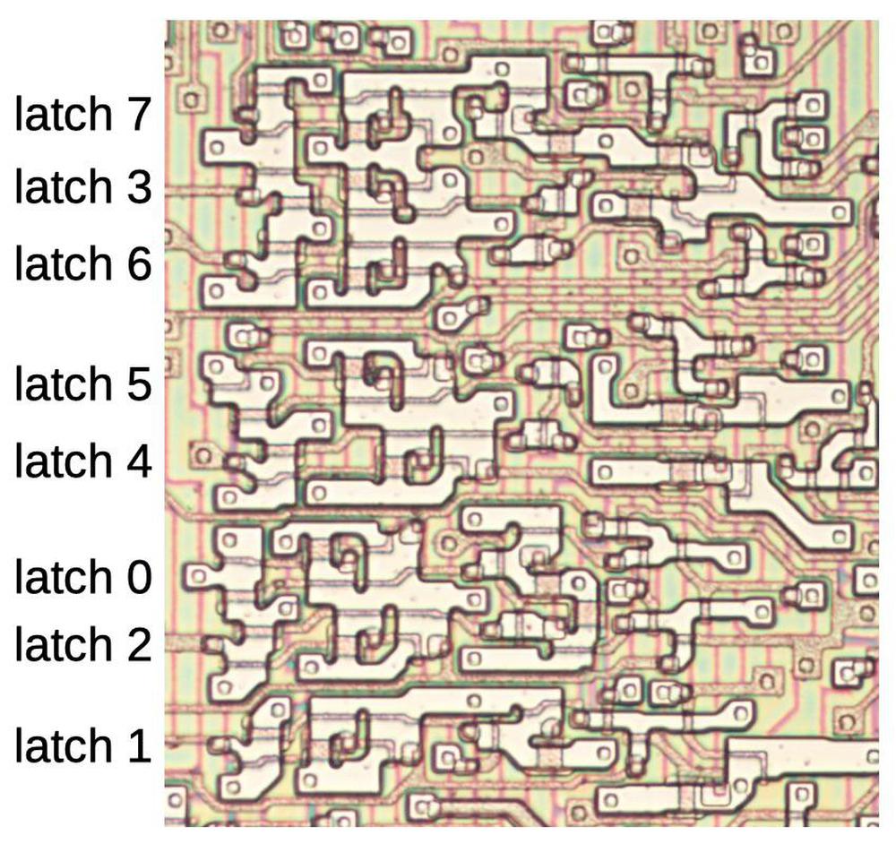
The 8086, like most processors, has an instruction register that holds the instruction that is currently being executed. In the 8086, the instruction register holds the first byte of an instruction (which may consist of multiple bytes), so it is built from eight latches (below). You might expect the latches to be identical, but each latch has a different shape. Since the layout of the 8086 is highly optimized, each latch is shaped to make the best use of the available space, constrained by the neighboring wiring. In particular, note that some latches are merged together so they can share power and ground connections. Layout optimization is also probably why the latches are not in sequential order.
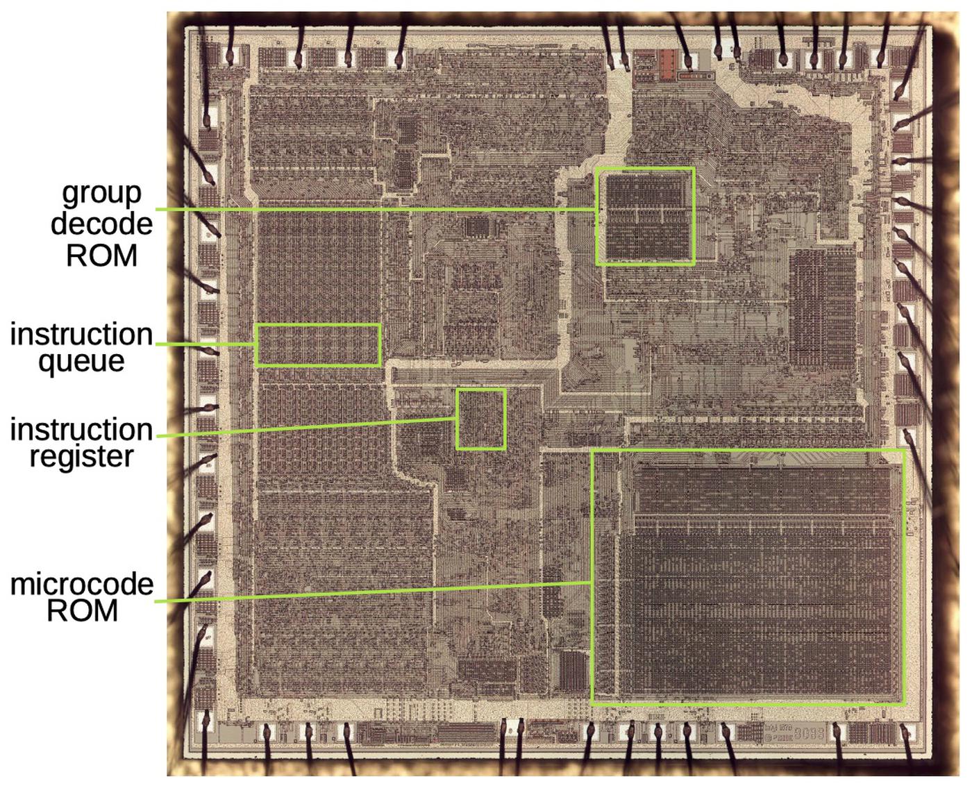
An instruction takes a winding journey through the 8086 chip. The 8086 processor uses prefetching, improving performance by loading instructions from memory before they are required. Prefetched instructions are stored in the instruction queue, a 6-byte queue in the middle of the 8086's register file. (In comparison, modern processors can have megabytes of instruction cache.) When an instruction is executed, it is stored in the instruction register, roughly in the middle of the chip. (The relatively large distances explains the use of superbuffers.) The instruction register feeds the instruction to the "group decode ROM". This ROM determines the high-level characteristics of the instruction, such as if it is a single-byte instruction, a multi-byte instruction, or an instruction prefix. (This is only a piece of the 8086's complex instruction handling. Other latches hold pieces of the instruction indicating register usage and the ALU operation, while a separate circuit controls the microcode engine, but I'll discuss that in another post.)
Conclusions
The 8086 makes extensive use of dynamic latches to store state internally. These latches are visible under a microscope and their circuitry can be traced out and understood. The 8086 is an interesting subject for die analysis since unlike modern processors, its transistors are large enough to see under a microscope, unlike modern processors. It was a complex processor at the time, with 29,000 transistors, but it is still simple enough that the circuitry can be traced out and understood.
I've written multiple posts about the internals of the 8086 processor lately. I plan to analyze the 8086 in more detail in future blog posts so follow me on Twitter @kenshirriff or RSS for updates.
Notes and references
-
The 8086 has over 80 latches. Some latches hold values for the AD (address/data) pins or control pins. Other latches hold the current microcode address and the microinstruction, as well as the return address for a microcode subroutine call. Other latches hold the source and destination register bits from the instruction, and the ALU operation from the instruction. Many latches hold internal state values that I'm still investigating. ↩
-
Many microprocessors use cross-coupled NOR (or NAND) gates to form an SR latch. An SR latch typically takes up more space than a dynamic latch, especially if additional circuity is added to make it clocked. Edge-triggered flip flops are popular, but are even more complex, using six gates. In many cases, a pass transistor provides sufficient storage; it can hold a value across a clock cycle, but doesn't provide the long-term storage of a latch. ↩
-
Processors always have a maximum clock speed, the fastest they can run. (The original 8086 ran at up to 5 MHz, while the later 8086-1 supported 10 MHz.) However, due to the use of dynamic logic, the 8086 also had a minimum clock speed of 2 MHz. If the clock ran slower than that, there was a risk of the charge on a wire leaking away before it was used, causing errors. ↩
-
A key to the operation of the latch is that there are two inverters, so the output is stable. An odd number of inverters would result in oscillation, a feature used by the 8086's charge pump oscillator. The 8086's register file also uses pairs of inverters to store bits. However, in the register file, the two inverters are connected to each other directly, without the clocked pass transistors, resulting in storage that is more compact but more difficult to control. ↩
-
The pull-up resistor in an NMOS gate is implemented by a special transistor. The depletion-mode transistor acts as a resistor but is more compact and performs better than an actual resistor. ↩
-
Some more information on superbuffers. The problem with an NMOS inverter is that the pull-up resistor provides limited current. When outputting a 0, the transistor in an inverter pulls the output low quickly, with a relatively high current. However, when outputting a 1, the output is pulled high by the much weaker pullup resistor.
The superbuffer is somewhat like a CMOS inverter in that it has a pullup transistor and a pulldown transistor. The difference is that CMOS uses both PMOS and NMOS transistors, and the PMOS transistor has an inverted gate input. In contrast, with an NMOS superbuffer, a separate inverter is required. In other words, a CMOS inverter uses two transistors, while a superbuffer is much less efficient, requiring four transistors.
The superbuffer uses a depletion mode transistor for the pullup and an enhancement mode transistor for the pulldown. The depletion-mode transistor has a threshold voltage below zero, allowing its output (source) to get pulled up to 5V, rather than shutting off a bit lower. When the output is low, the depletion-mode transistor will still be (somewhat) on, acting like the pullup in a regular inverter, so there is some current flow through it. For more on superbuffers, see Introduction to VLSI Systems, page 28. ↩


I've been wanting to read about this for years, thanks!
ReplyDeleteI really want to read when you reach ALU decoding, and if possible microcode decoding (and a raw dump of it)
Many thanks for a great work.
Great article!
ReplyDeleteOne of the side effects of dynamic logic is that they often have a minimum operating frequency. This means you can't just stop the clock, or run the clock at a very slow rate. Sometimes its useful to slow down the clock when debugging a circuit, which allows for testing the logic without fully stressing the timing of the circuit. There are also reasons to stop the clock, which wasn't allowed.
NMOS logic took longer for a 0 to 1 transition than a 1 to 0 transition, especially on a bus, so dynamic circuits were sometimes used to precharge a bus to a 1 state before changing it to a 0 if required. This was very common in memory chips, which used a lot of analog circuits internally.
Are any of the 8086 designers still around? It'd be interesting to get their commentary on your detailed reverse engineering.
ReplyDeletethanks
ReplyDeleteTom
I worked for a small aerospace company in 1989 that based its satellite flight computer on a CMOS 8086 made my Harris. For power reasons, the CPU spent a lot of its time running at 256 kHz, with the clock bumped up to full speed (I forget the rate now) when it was time to do some real work. There were only two CPU emulators that supported that clock - one made by Zax (it was terrible) and the other by SoftAid, which was by far the best one I've ever worked with.
ReplyDeleteI expected the register flip-flops that you described earlier to be larger, and hence why they would go through the trouble of using dynamic latches. But from your notes, the dynamic latch is actually larger. Why did they use the dynamic latch then? Faster?
ReplyDelete