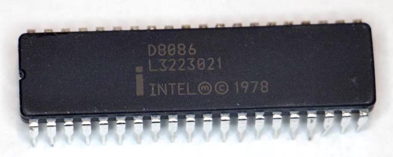
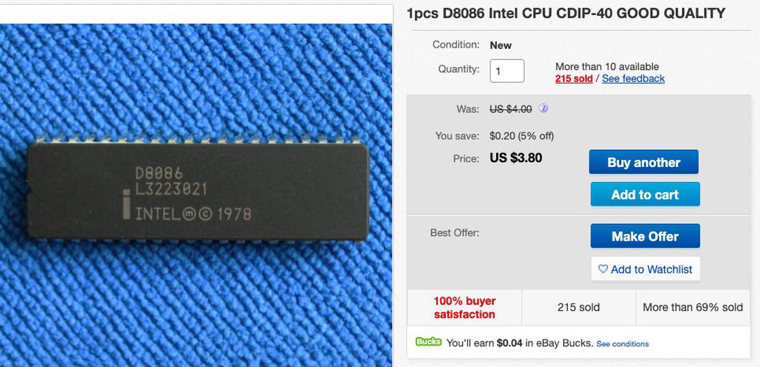
Intel introduced the 8086 processor in 1978, leading to the x86 architecture in use today. I'm currently reverse-engineering the circuitry of the 8086 so I've been purchasing vintage 8086 chips off eBay. One chip I received is shown below. From the outside, it looks like a typical Intel 8086.
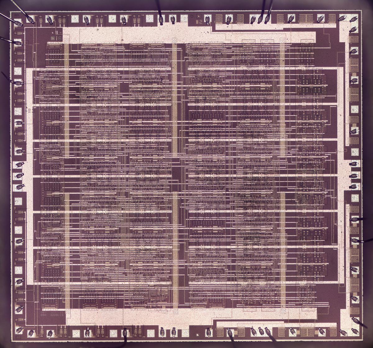
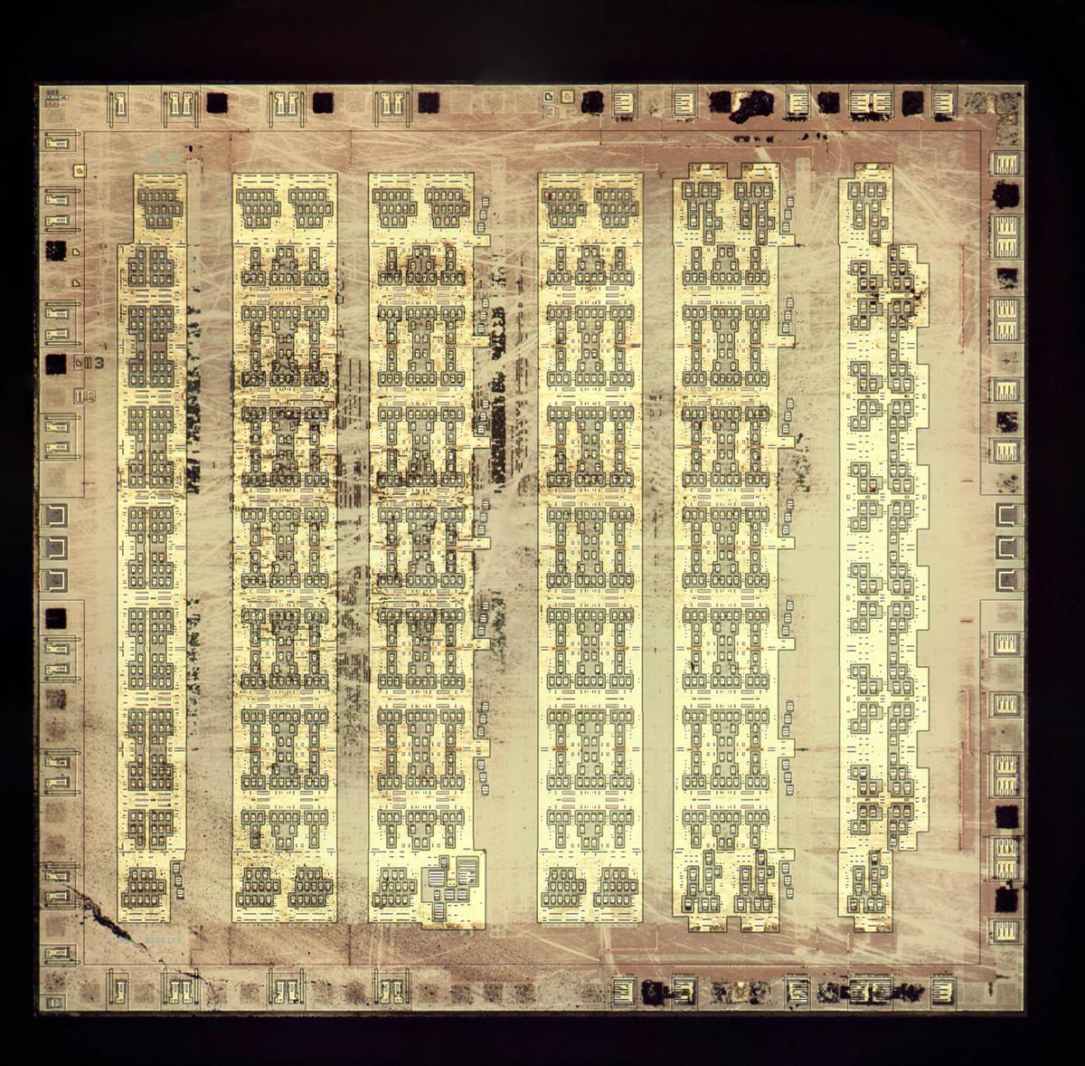
I opened up the chip and looked at it under the microscope, creating the die photo below. The whitish lines are the metal layer, connecting the chip's circuitry. Underneath, the silicon has a purple hue. Around the outside of the die, bond wires connect the square pads to the 40 external pins on the IC.
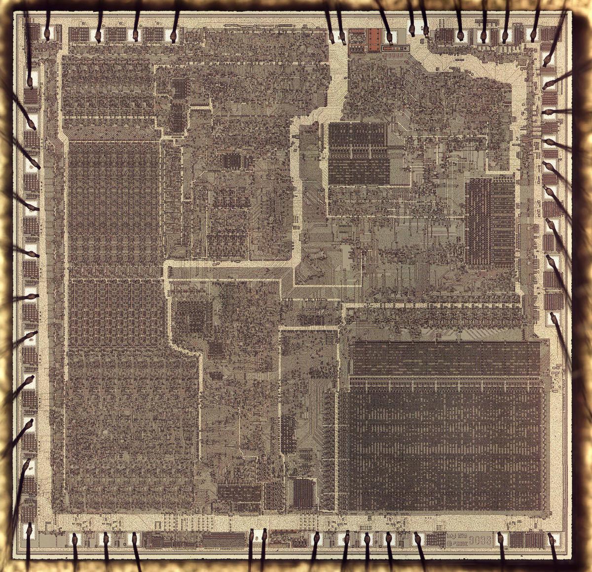
I quickly noticed, however, that this wasn't an 8086 processor but something entirely different! For comparison, look at my die photo of a genuine 8086 below. As you can see, the chips are entirely different and the 8086 is much more complex. Someone had taken a random 40-pin chip and relabeled it as an Intel 8086 processor. The genuine 8086 has various functional blocks visible: the 16-bit registers and ALU on the left, the large microcode ROM in the lower right, and various other blocks of circuitry throughout the chip. (The genuine chip also has a tiny Intel copyright and the 8086 part number in the lower right. Click the image to magnify.) The fake chip above, on the other hand, is an irregular grid of horizontal and vertical wiring, with thicker horizontal and vertical lines for power.
The ULA or Uncommitted Logic Array
If the chip isn't an 8086, what is it? I believe the fake chip is an Uncommitted Logic Array, a type of gate array. A gate array is a way of making semi-custom integrated circuits without the expense of a fully-custom design. The idea behind a gate array is that the silicon die has a standard array of transistors that can be wired up to create the desired logic functions. This wiring is done in the chip's metal layers, which are designed for the customer's requirements.2 Although a gate array doesn't provide the flexibility of a fully-custom design, it was considerably cheaper and faster to design.
Ferranti invented the ULA in 1972, claiming that it was the first "to turn the logic array concept into a practical proposition." A ULA allowed a single LSI chip to replace hundreds or even thousands of gates that otherwise would be implemented in a board full of 7400-series TTL chips. The most well-known users of a ULA are the popular Sinclair ZX 81 and ZX Spectrum home computers.3
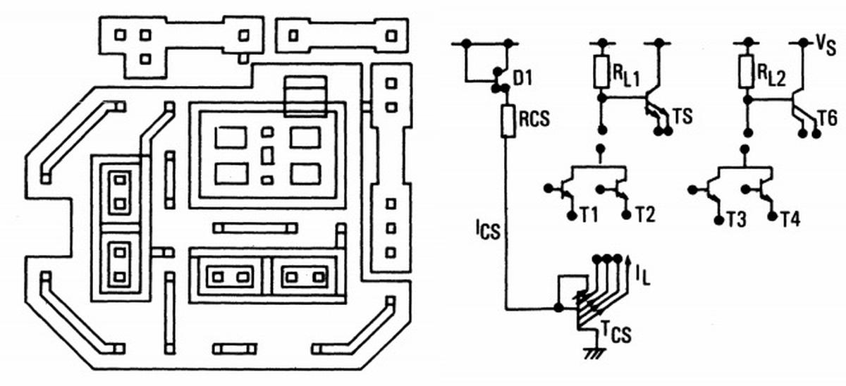
A ULA was based on a matrix of identical cells that were wired to form the logic gates. Around the edges of the chip, standardized peripheral cells provided the desired I/O capabilities. The diagram below shows a typical cell in the matrix. The cell contains multiple transistors and resistors, which are mostly unconnected by default. The ULA is customized by creating connections between the components to build a set of logic gates.
The photo below shows the fake chip with the metal layers removed, revealing the transistor array underneath. Each small green/yellow rectangle is a transistor; there are nearly 1000 of them. Note the repeated pattern of cells in the matrix,1 as well as the different peripheral cells around the outside. The density of transistors is fairly low; the chip has empty columns to provide room to route the metal layer.
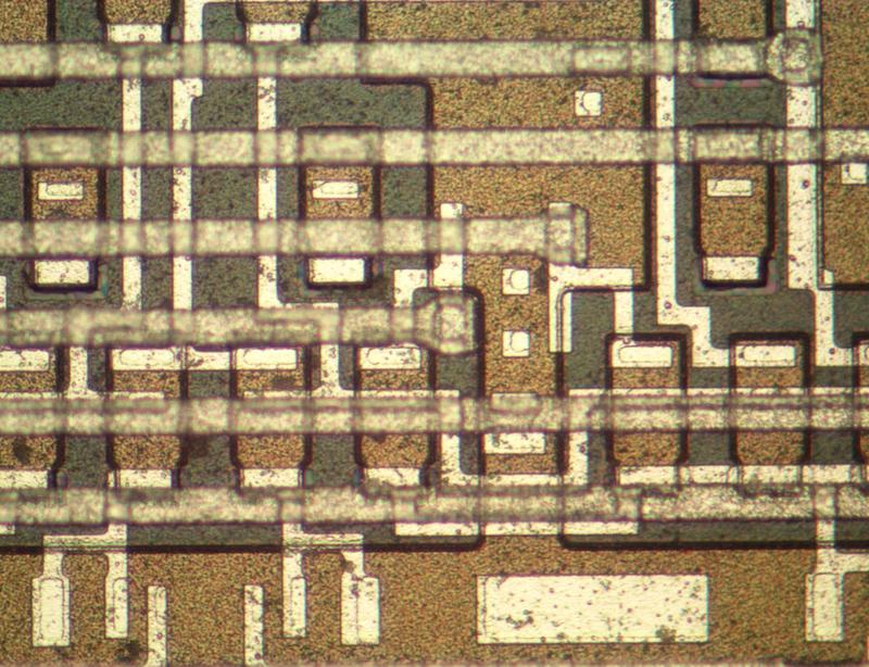
The fake chip uses bipolar transistors,4 completely different from the NMOS transistors in the 8086 processor. The closeup below shows transistors (the striped rectangles) and the two layers of metal wiring connecting them. (The genuine 8086 only has one metal layer, so the fake chip is probably more recent, from the 1980s.)
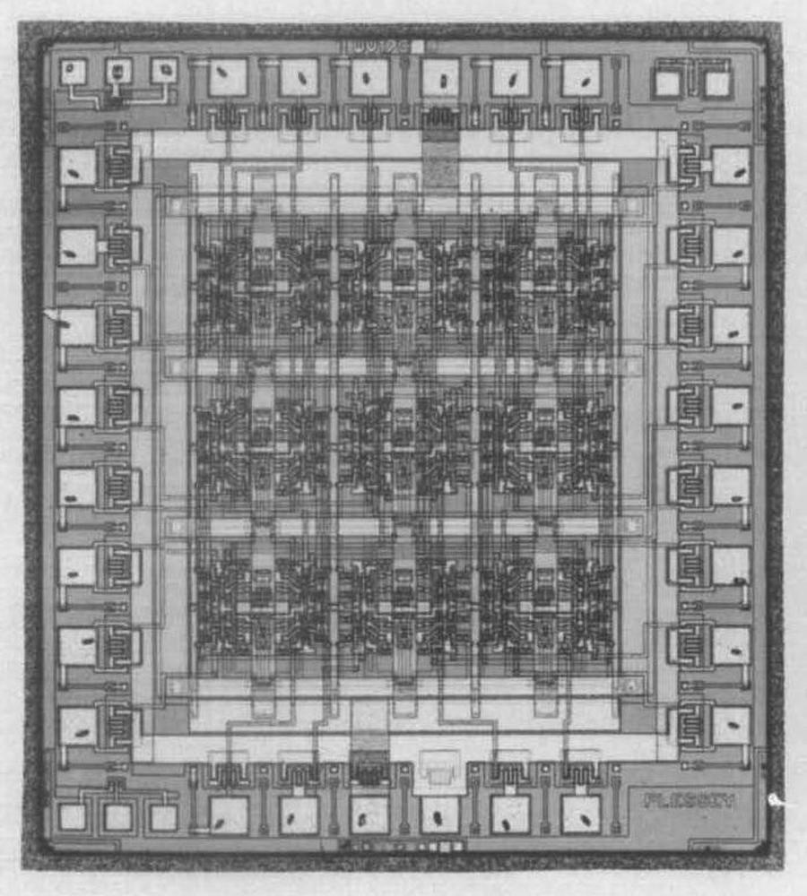
There is no manufacturer printed on the die of the fake chip. The matrix cells don't look like the Ferranti cells. The photo below shows a ULA built by Plessey, another ULA manufacturer. That die has a smaller transistor matrix than my chip, but the overall structure is roughly similar, so Plessey might be the manufacturer.
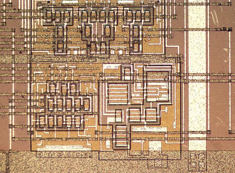
The photo below shows another detail of the fake chip. Matrix cells are at the top. The peripheral cell below has much larger transistors for I/O. (There are also resistors in the brownish regions, but they aren't really visible.) The upper metal layer consists of horizontal wiring, while the lower metal layer is mostly vertical. The thick metal line at the right is for power (or perhaps ground) and is connected to a horizontal power distribution trace at the bottom.
To summarize, the position of the transistors and resistors in the ULA is fixed. This allows the same underlying silicon wafers to be manufactured for all the customers, keeping volume high and costs low. But by customizing the metal wiring layers, the ULA can be completed to fulfill the logic functions each customer needs.
Conclusions
Why would someone go to all the work of relabeling a $3.80 chip? I guess someone had a stack of old custom ICs with no value. By re-labeling them, they could at least get something for them. It hardly seems worth the effort, but I guess they make up for it in volume. The seller has sold over 215 of these 8086's, although I don't know if they were all fake or if I was unlucky. In any case, the seller gave me a prompt refund.
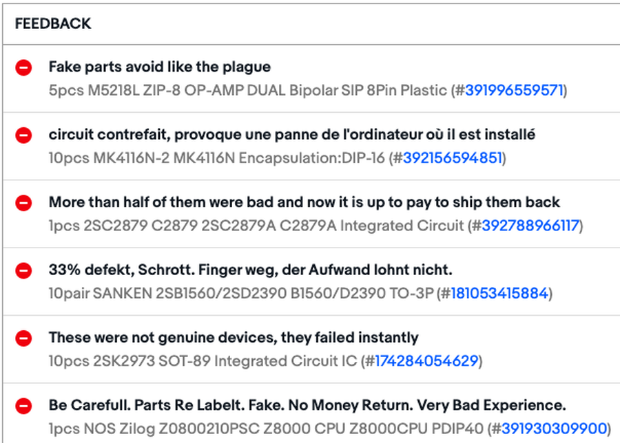
The seller's feedback (below) shows a lot of complaints about fake chips. Even so, the seller's feedback is 99.2% positive, so I suspect that there are just a few fake chips mixed in with many types of real chips. It's also possible that most vintage 8086s are purchased by IC collectors who never test the chip.
I've been asked if this chip would actually work as an 8086. Sometimes counterfeiters sell a lower-quality chip in place of the real thing, such as the fake expensive op amps found by Zeptobars. But other times the fake chip is unrelated, such as the vintage bipolar RAM chips that I determined was a Touch-Tone dialer. Since an 8086 has 29,000 MOS transistors but the fake chip has under 1000 bipolar transistors, it's clear that this chip won't function as an 8086.
The moral is to always be careful when you're buying chips, since you never know what you might find. Semiconductor counterfeiting is a big business and I've encountered just a tiny piece of it. I plan to write more about reverse-engineering the (real) 8086, so follow me on Twitter at @kenshirriff for updates. I also have an RSS feed.
Notes and references
-
I think the fake chip has a matrix of 8×12 cells, with each of the large "IXI" patterns composed of four cells. ↩
-
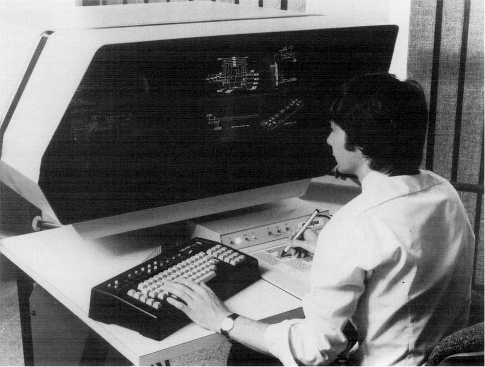
At first, a ULA was designed by hand by an engineer drawing the interconnects on paper, but by the 1980s, CAD software automated most of the design and testing. The CAD station below is pretty wild.
CAD system for designing ULAs at Plessey. From "Computer Aided Design and New Manufacturing Methods for Electronic Materials", 1985. -
The book The ZX Spectrum ULA: How to design a microcomputer discusses Ferranti ULAs in detail along with a complete explanation of the ULA in the ZX Spectrum. ↩
-
Early ULAs used bipolar transistors, with CMOS circuitry introduced later. Different logic families were supported, depending on the needs of the application. Ferranti's ULAs had three types of matrix cells: RTL (resistor-transistor logic), CML (current-mode logic), and buffered current-mode logic. Other ULAs supported fast ECL (emitter-coupled logic) or standard TTL (transistor-transistor logic). ↩
Plessey took over Ferranti. I used to work there in the late 80s/early 90s and we were still making ULA based devices. I don't remember them making this one though.
ReplyDeleteGive him a solid negative review and open a case on eBay, pointing them to this article. The seller should be removed.
ReplyDeleteSeller may not have known and bought these old chips in bulk - if they haven't the hardware to test, how would you shift the right chips (pun intended)?
DeleteWhat could this have been used for?
ReplyDeleteThe CAD workstation looks like a GE Calma machine based on a Data General 16 bit computer. Calma pioneered the GDSII (Graphic Design System) format to represent the CAD mask layers of a chip. Not all layers had to be digitized as some could be created as logical combinations of the digitized layer during the 'stream out' process. This is the format still used today to transfer chip databases before 'fracturing' into the MEBES format used to drive the electron beams that print the masks. The graphics system had a an assembly-like language called GPLII. Mostly it was used for small functions like converting text like "8086" into geometric shapes that could be printed as polysilicon or metal on the chip. But we actually wrote pretty complex programs in GPLII to automate the I/O, pad, and core cell placement or gate arrays of various sizes. The predecessor of todays automatic place and route programs. The giant touch pad and wired pen is still the best and most precise computer interface I've ever used.
ReplyDeleteMy first ever eBay purchase - in 1996 - was a motherboard. It turned out to have fake L2 cache ram soldered to the board! These were hard wired chips with DIP SRAM pin-outs wired to simply always report a cache miss. (ironically increasing memory latency even more than not having a cache at all; but the manufacturer sure made a killing off these given memory prices at the time)
ReplyDeleteThe seller in my case was some fly by night would be computer shop owner in Texas who didn't last long. I'm not sure if he was aware of the scam or also a victim, but his behavior at the time made it clear he wasn't happy with the results... ;)
Someone appears to have documented these boards: https://www.redhill.net.au/b/b-bad.html
Counterfeits in hardware... a regularly recurring theme. So much value in a tiny package it is bound to happen. A fake CPU that can't even pretend to work though? That is just odd!
Ken,
ReplyDeletelove your work !
I worked on Ferranti CML ULA in the early 80's. We used a dec microvax, with one graphics terminal we shared (had a sign up sheet!) , several text only terminals and a large tablet for coordinate input. We did not use calma. Not saying others did not, just that we did not at that time.
There were several ferranti CML family variants at that time, all single layer metal. I do have some old pics, plots and marketing flier material, I should scan and put on the internet for historical purposes.(Once I get back to the office)
In another job (later) we used Calma, and Daisy for capturing Gate array logic and layout. (Plessy, Ti and Japanese suppliers).
Being a total noob, I really admire what you are doing here. It really blows my mind.
ReplyDeleteWhat I asked myself (and - without result - Google):
Destructive testing if a chip is counterfeit or not is not really feasible if you potentially want to use the chip for whatever purpose (be it just for having it in a collection of chips).
Is there a broadly usable method of testing chips if they are counterfeit or not without having to be a specialist with your knowledge and destroying the chip? Maybe with a opensource test-sequence via connecting an ESP32?
That CAD workstation is in deed a Calma machine. Calma was started in sunnyvale in the 60's by husband and wife Calvin and Irma (CalMa is a contraction). The machine was called a GDS : graphic Design System and had a proprietary operating system and data format GDS Stream format. Version 2 (GDS-II) of that format is still in use today for mask making for integrated circuits. The machine was essential a Data General Nova with a Hazeltine terminal and a second graphics display. The whole thing is purely a vector based drawing system originally designed to make geographic drawings. The general purpose vector operations could be used to build anything and it was soon discovered that this was ideal to make chip layout. By the late 70's every semiconductor manufacturer in the world was running on these things. I used one in the early 90's.
ReplyDeleteThere is a movie (Brainstorm) where they use one of these systems. It was very impressive for 1970's technology. https://www.youtube.com/watch?v=pDi7N2a41Fk
As for the ULA : that looks like an AMI 10000 or earlier series sea-of-gates array. it could be an IIL (integrated injection logic) array. Those were Signetics i believe.
I used the Calma workstations in the mid-80's to push polygons. This was in the days before automatic place and route. I wrote a program in the GPLII language that was a crude place and route program. It took a text file as input that specified the die size and list of I/O and power pins. The output was a Calma database with all the I/O and pad cells placed. Save a ton of manual work.
ReplyDeleteIn responce to the question about non destructive testing for a simple test you could use a
ReplyDeletemethod like Here modified for the 8086.
For a more in depth test i suggest connecting it to a raspberry pi see here.
hope this helps.