Inside the 8086 processor, tiny charge pumps create a negative voltage

Introduced in 1978, the revolutionary Intel 8086 microprocessor led to the x86 processors used in most desktop and server computing today. This chip is built from digital circuits, as you would expect. However, it also has analog circuits: charge pumps that turn the 8086's 5-volt supply into a negative voltage to improve performance.1 I've been reverse-engineering the 8086 from die photos, and in this post I discuss the construction of these charge pumps and how they work.

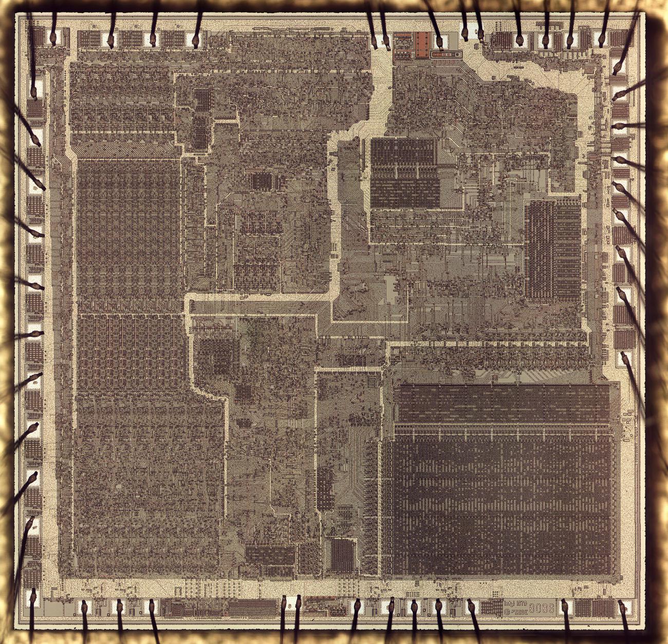
Die photo of the 8086 microprocessor. The ALU and registers are on the left. The microcode ROM is in the lower right. Click for a high-resolution image.

Die photo of the 8086 microprocessor. The ALU and registers are on the left. The microcode ROM is in the lower right. Click for a high-resolution image.

The photo above shows the tiny silicon die of the 8086 processor under a microscope. The metal layer on top of the chip is visible, with the silicon hidden underneath. Around the outside edge, bond wires connect pads on the die to the chip's 40 external pins. However, careful examination shows that the die has 42 bond pads, not 40. Why are there two extra ones?

An integrated circuit starts with a silicon substrate, and transistors are built on this. For high-performance integrated circuits, it is beneficial to apply a negative "bias" voltage to the substrate. 2 To obtain this substrate bias voltage, many chips in the 1970s had an external pin that was connected to -5V,3 but this additional power supply was inconvenient for the engineers using these chips. By the end of the 1970s, however, on-chip "charge pump" circuits were designed that generated the negative voltage internally. These chips used a single convenient +5V supply, making engineers happier.

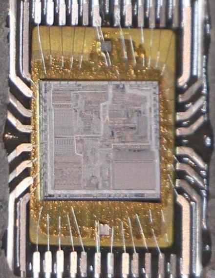
A closeup of the 8086 chip showing the silicon die and the bond wires connecting it to the lead frame.

A closeup of the 8086 chip showing the silicon die and the bond wires connecting it to the lead frame.

On the 8086 die, the two extra pads feed this negative bias voltage to the substrate. The photo above shows the silicon die as mounted in the chip, with bond wires connected to the lead frame that forms the pins. Looking carefully, there are two small gray squares above and below the die; each connected to one of the "extra" bond pads. The charge pumps on the 8086 die generate a negative voltage, which passes through the bond wires to these squares, and then through the metal plate underneath to the 8086's substrate.

How the charge pumps work

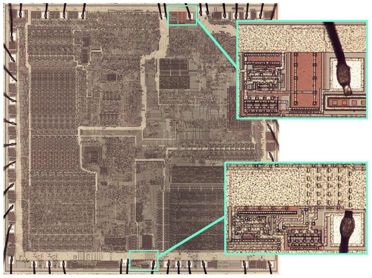
The photo below highlights the two charge pumps in the 8086. I'll discuss the top one; the bottom one has the same circuitry but a different layout to fit in the available space. Each pump has driver circuitry, a large capacitor, and a pad with the bond wire to the substrate. Each pump is located next to one of the 8086's two ground pads, presumably to minimize electrical noise.

Die photo of the 8086 microprocessor, zooming in on the two substrate bias generators.

Die photo of the 8086 microprocessor, zooming in on the two substrate bias generators.

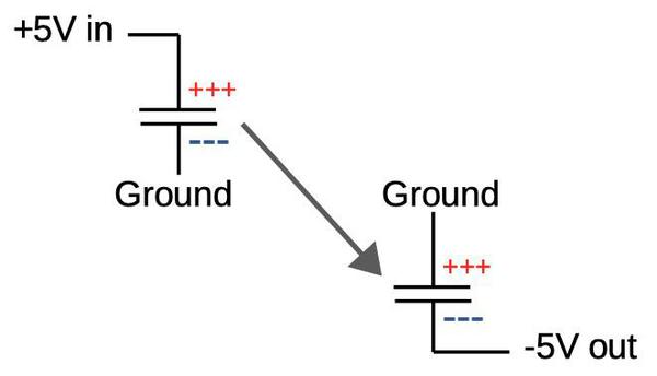
You might wonder how a charge pump can turn a positive voltage into a negative voltage. The trick is a "flying" capacitor, as shown below. On the left, the capacitor is charged to 5 volts. Now, disconnect the capacitor and connect the positive side to ground. The capacitor still has its 5-volt charge, so now the low side must be at -5 volts. By rapidly switching the capacitor between the two states, the charge pump produces a negative voltage.

On the left, the "flying capacitor' is charged to 5 volts. By switching ground to the upper terminal, the capacitor now outputs -5 volts. (source)

On the left, the "flying capacitor' is charged to 5 volts. By switching ground to the upper terminal, the capacitor now outputs -5 volts. (source)

The 8086's charge pump circuit uses MOSFET transistors and diodes to switch the capacitor between the two states, with an oscillator to control the transistors, as shown in the schematic below. The ring oscillator consists of three inverters connected in a loop (or ring). Because the number of inverters is odd, the system is unstable and will oscillate.5 For instance, if the input to the first inverter is 0, its output will be 1, the second output will be 0, and the third output will be 1. This will flip the first inverter, and the "flip" will travel through the loop causing oscillation. To slow down the oscillation rate, two resistor-capacitor networks are inserted into the ring. Since the capacitors will take some time to charge and discharge, the oscillations will be slowed, giving the charge pump time to operate.4

Schematic of the charge pump used in the Intel 8086 to provide negative substrate bias.

Schematic of the charge pump used in the Intel 8086 to provide negative substrate bias.

The outputs from the ring oscillator are fed to the transistors that drive the capacitor. In the first step, the upper transistor is switched on, causing the capacitor to charge through the first diode to 5 volts with respect to ground. The second step is where the magic happens. The lower transistor turns on, connecting the high side of the capacitor to ground. Since the capacitor is still charged to 5 volts, the low side of the capacitor must now be at -5 volts, producing the desired negative voltage. This goes through the second diode and the bond wire to the substrate. When the oscillator flips again, the upper transistor turns on and the cycle repeats. The charge pump gets its name because it pumps charge from the output to ground.6 The diodes are similar to check valves in a water pump, making sure charge moves in the right direction.

The implementation in silicon

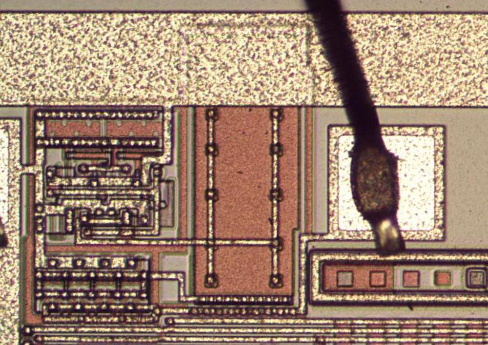
The photo below shows the charge pump as it is implemented on the chip. In this photo, the metal wiring is visible on top, with reddish polysilicon underneath and beige silicon at the bottom. The main capacitor is visible in the center, with H-shaped wiring connecting it to the circuitry on the left. (Part of the capacitor is hidden under the wide metal power trace at the top.) On the right, the substrate bond wire is attached to the pad. A test pattern is below the pad; it has a square for each mask used to produce a layer of the chip.

The charge pump, showing the metal layer.

The charge pump, showing the metal layer.

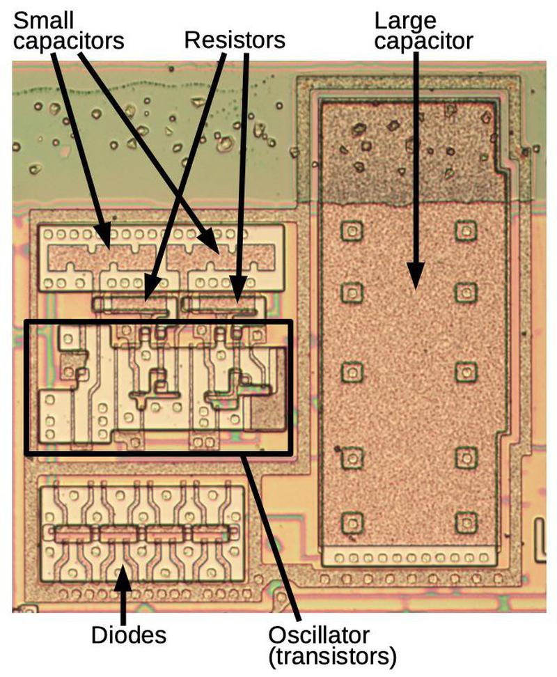
Removing the metal layer shows the circuitry more clearly, below. The large charge pump capacitor takes up the right half of the photo. Although microscopic, this capacitor is huge by chip standards, about the size of a 16-bit register. The capacitor consists of polysilicon over a silicon region, separated by insulating oxide; the polysilicon and silicon form the plates of the capacitor. On the left side are the smaller capacitors and the resistors that provide the R-C delay for the oscillator. Below them is the oscillator circuitry and the drive transistors.7

An 8086 charge pump, showing the key components. The metal has been removed for this photo, to show the silicon and polysilicon underneath.

An 8086 charge pump, showing the key components. The metal has been removed for this photo, to show the silicon and polysilicon underneath.

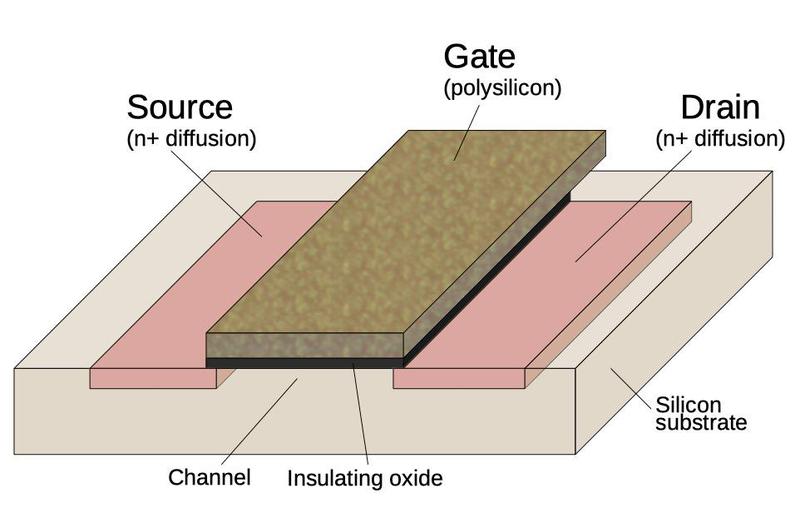
One interesting feature of the charge pump is the two diodes, each built from eight transistors in a regular pattern. The diagram below shows the structure of a transistor. Regions of the silicon are doped with impurities to create diffusion regions with desired properties. The transistor can be viewed as a switch, allowing current to flow between two diffusion regions called the source and drain. The transistor is controlled by the gate, made of a special type of silicon called polysilicon. A high voltage on the gate lets current flow between the source and drain, while a low voltage blocks current flow. These tiny transistors can be combined to form logic gates, the components of microprocessors and other digital chips. But in this case, the transistors are used as diodes.

Structure of an NMOS transistor (MOSFET) as implemented in an integrated circuit.

Structure of an NMOS transistor (MOSFET) as implemented in an integrated circuit.

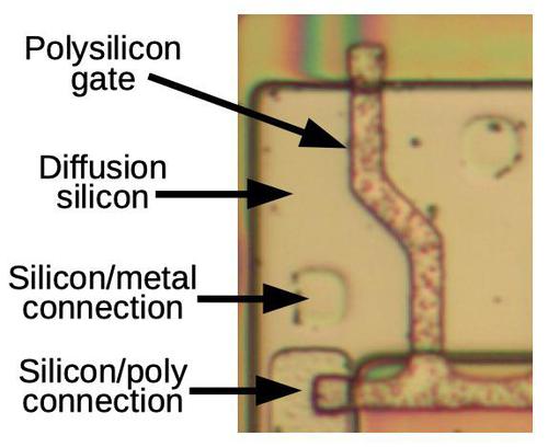
The photo below shows a transistor in the charge pump, viewed from above. As in the diagram, polysilicon forms the gate between the silicon diffusion regions on either side. A diode can be formed from a MOSFET by connecting the gate and drain together (details) through the silicon/polysilicon connection at the bottom of the photo. The silicon can also be connected to the metal layer through a "via". The metal layer was removed for this photo, but faint circles indicate the position of silicon/metal vias.

A transistor in the charge pump circuit. The polysilicon gate separates the transistor's source and drain on either side.

A transistor in the charge pump circuit. The polysilicon gate separates the transistor's source and drain on either side.

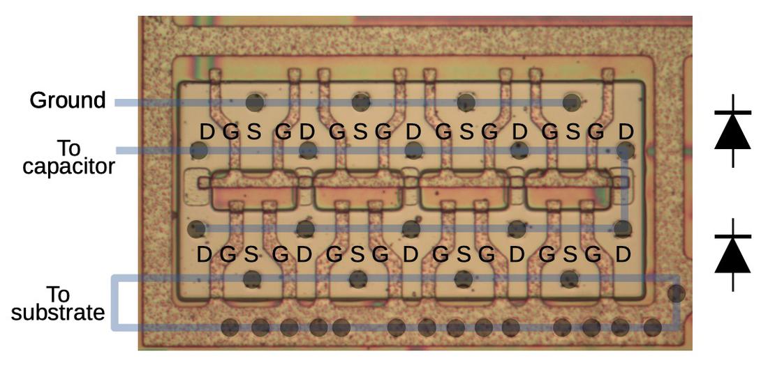
The diagram below shows how the two diodes are implemented from 16 transistors. To support the relatively high current of the charge pump, eight transistors are used in parallel for each diode. Note that neighboring transistors share source or drain regions, allowing transistors to be packed densely. The blue lines indicate the metal wires; the metal was removed for this photo. The dark circles indicate connections (vias) between the metal and silicon.

The charge pump has two diodes, each implemented with 8 transistors. The source, gate, and drain are indicated with S, G, and D.

The charge pump has two diodes, each implemented with 8 transistors. The source, gate, and drain are indicated with S, G, and D.

Putting this all together, the upper eight transistors have their sources connected to ground by a metal wire. Their gates and drains connected together by the polysilicon below the transistors, making them into diodes, and they are connected to the capacitor by a metal wire. The lower eight transistors form a second diode; their gates and drains are wired together by the lower metal wire loop. Note how the layout has been optimized; for example, the gates have bent shapes to avoid the vias (black dots).

Conclusions

The substrate bias generator on the 8086 chip9 is an interesting combination of digital circuitry (a ring oscillator formed from inverters) and an analog charge pump. While the bias generator may seem like an obscure part of 1970s computer history, bias generation is still part of modern integrated circuits. It is much more complex in modern chips which have multiple carefully regulated biases in multiple power domains. 8 In a sense it is analogous to the x86 architecture, something that started in the 1970s and is even more popular today, but has become unimaginably more complex in the quest for higher performance.

If you're interested in the 8086, I wrote about the 8086 die, its die shrink process and the 8086 registers earlier. I plan to analyze the 8086 in more detail in future blog posts so follow me on Twitter @kenshirriff or RSS for updates.

Notes and references

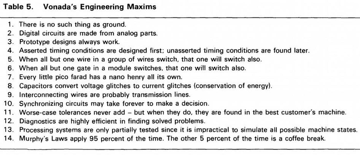
  1. Strictly speaking, the entire chip is analog: there's an old saying that "Digital computers are made from analog parts". This saying came from DEC engineer Don Vonada and was published in DEC's Computer Engineering in 1978.

    Vonada's Engineering Maxims (text).

    Vonada's Engineering Maxims (text).


  2. Putting a negative bias voltage on the substrate had several benefits. It decreased parasitic capacitance making the chip faster, made the transistor threshold voltage more predictable, and reduced leakage current

  3. Early DRAM memory chips and microprocessor chips often required three supplies: +5V (Vcc), +12V (Vdd) and -5V (Vbb) bias voltage. In the late 1970s, improvements in chip technology allowed a single supply to be used instead. For example, Mostek's MK4116 (a 16 kilobit DRAM from 1977) required three voltages while the improved MK4516 (1981) operated on a single +5V supply, simplifying hardware designs. (Amusingly, some of these chips still kept the Vbb and Vcc pins for backward compatibility but left them unconnected.) Intel's memory chips followed a similar path, with the 2116 DRAM (16K, 1977) using three voltages and the improved 2118 (1979) using a single voltage. Similarly, the famous Intel 8080 microprocessor (1974) used enhancement-mode transistors and required three voltages. An improved version, the 8085 (1976), used depletion-mode transistors and was powered by a single +5V supply. The Motorola 6800 microprocessor (1974) used a different approach for a single supply; although the 6800 was built from the older enhancement-load transistors it avoided the +12 supply by implementing an on-chip voltage doubler, a charge pump that increased the voltage. 

  4. I tried to measure the frequency of the charge pump by looking at the chip's current to see fluctuations due to the charge pump. I measured 90 MHz fluctuations, but I suspect I was measuring noise and not the charge pump's oscillations. 

  5. Because the circuit has an odd number of inverters, it oscillates. If, on the other hand, it had an even number of inverters, it would be stable in two different states. This technique is used in the 8086's registers: a pair of inverters stores each bit (details). 

  6. I've simplified the charge pump discussion slightly. Due to voltage drops in the transistors, the substrate voltage will probably be around -3V, not -5V. (If a chip requires a larger voltage drop, charge pump stages can be cascaded.) For the pump direction, I'm referring to current flow. If you think of it as pumping electrons, the negative electrons are being pumped the opposite direction, into the substrate. 

  7. The oscillator is built from 13 transistors. Seven transistors form the 3 inverters (one inverter has an extra transistor to provide extra output current. The six drive transistors consist of two transistors pulling the output high and four transistors pulling the output low. The layout is strangely different from normal inverter circuitry, probably because the current requirements are different from normal digital logic. 

  8. Bias generators are now available as IP blocks that can be licensed and be plugged into a chip design. For more information on bias in modern chips, see Body bias, Multi bias domain implementation, or this presentation. There is even a standard IEEE 1801 power format that allows IC design tools to generate the necessary circuitry. 

  9. The Intel 8087, the math coprocessor chip that goes along with the 8086, also has a substrate bias generator. It uses the same principles, but unexpectedly has a different circuit, using 5 inverters. I wrote about it in detail here

The Intel 8086 processor's registers: from chip to transistors

The Intel 8086 microprocessor is one of the most influential chips ever created; it led to the x86 architecture that dominates desktop and server computing today. I've been reverse-engineering the 8086 from die photos, and in this post I discuss how its register file is implemented.

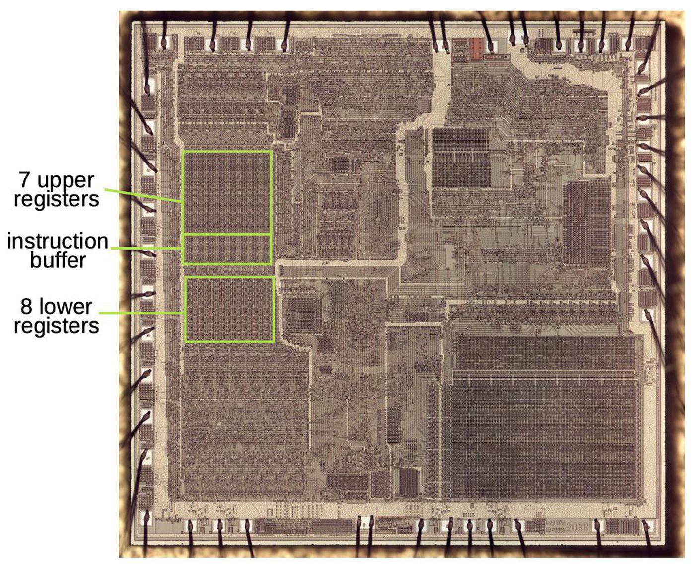
The 8086 die, showing the register storage. The upper registers are used by the Bus Interface Unit for memory accesses,
while the general-purpose lower registers are used by the Execution Unit. The instruction buffer is a 6-byte queue of prefetched
instructions.

The 8086 die, showing the register storage. The upper registers are used by the Bus Interface Unit for memory accesses, while the general-purpose lower registers are used by the Execution Unit. The instruction buffer is a 6-byte queue of prefetched instructions.

The photo above shows the silicon die of the 8086 processor under a microscope. The metal layer on top of the chip is visible, with the silicon hidden underneath. Around the outside edge, bond wires connect pads on the die to the chip's 40 external pins.

The highlighted region indicates the 8086's fifteen 16-bit registers and six bytes of instruction prefetch queue.1 Registers take up a significant portion of the die, even though they are just 36 bytes in total. Due to space limitations, early microprocessors had a relatively small number of registers; in comparison, a modern processor chip has kilobytes of registers and megabytes of cache storage.2

How a register is implemented in silicon

I'll start by explaining how the 8086 is built from NMOS transistors. Then I'll explain how an inverter is constructed, how a single bit is stored using inverters, and how a register is constructed.

The 8086 and other chips of that era were built from a type of transistor called NMOS. These chips consisted of a silicon substrate, which was "doped" by diffusion of arsenic or boron to form transistors. Above the silicon, polysilicon wiring created the gates of the transistors and wired components together. Finally, a metal layer on top provided more wiring. (Modern processors, in comparison, use CMOS technology, which combines NMOS and PMOS transistors, and they have many metal layers.)

The schematic below shows an inverter built from an NMOS transistor and a resistor3 With a low input, the transistor is off, so the pull-up resistor pulls the output high. With a high input, the transistor turns on, connecting ground and the output, pulling the output low. Thus, the input signal is inverted.

This schematic shows how an inverter is created from a transistor and resistor. The photo shows the implementation on the chip.
The metal layer was removed to show the polysilicon and silicon underneath.

This schematic shows how an inverter is created from a transistor and resistor. The photo shows the implementation on the chip. The metal layer was removed to show the polysilicon and silicon underneath.

The photo above shows how an inverter is physically constructed in the 8086. The pinkish regions are conductive doped silicon and the sparkly copper-colored lines are polysilicon on top. A transistor is created where polysilicon crosses silicon: the polysilicon forms the transistor's gate, while the silicon regions on either side are the transistor's source and drain. The large polysilicon rectangle forms the pull-up resistor between +5 volts and the output. Thus, the chip's circuitry matches the inverter schematic. Under a microscope, circuits such as this inverter are visible and can be reverse-engineered.

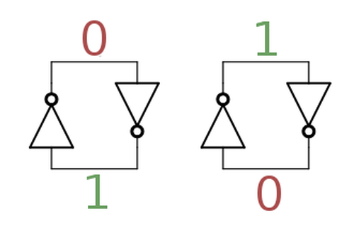
The building block for the registers is two inverters in a feedback loop, storing a single bit, as shown below. If the top wire has a 0, the right inverter will output a 1 to the bottom wire. The left inverter will then output a 0 to the top wire, completing the cycle. Thus, the circuit is stable and will "remember" the 0. Likewise, if the top wire is a 1, this will get inverted to a 0 at the bottom wire, and back to a 1 at the top. Thus, this circuit can store either a 0 or a 1, forming a 1-bit memory.

In the 8086, two coupled inverters hold a single bit in the register. This circuit is stable in either the 0 or 1 state.

In the 8086, two coupled inverters hold a single bit in the register. This circuit is stable in either the 0 or 1 state.

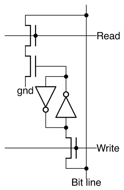
Three transistors are added to make a usable register cell from the inverter pair.4 One transistor selects the cell for reading, another transistor selects the cell for writing, and the third amplifies the signal when reading. In the center of the schematic below, two inverters store the bit. To read the bit, the read line is energized. This connects the inverter output to the bit line through the amplifying transistor. To write the bit, the write line is energized, connecting the bit line to the inverters. By putting a high-current 0 or 1 signal on the bit line, the inverters (and thus the stored bit) are forced to the desired value. Note that the bit line is used for both reading and writing.

Schematic diagram of a register cell storing a single bit. The register file is built from an array of these cells.

Schematic diagram of a register cell storing a single bit. The register file is built from an array of these cells.

The register file consists of a matrix of register cells like the one above. The matrix is 16 cells wide since registers are 16 bits wide. Each register is arranged horizontally, so a read line or write line select all the cells for a particular register. The 16 vertical bit lines form a bus, so all 16 bits in the selected register are read or written in parallel.

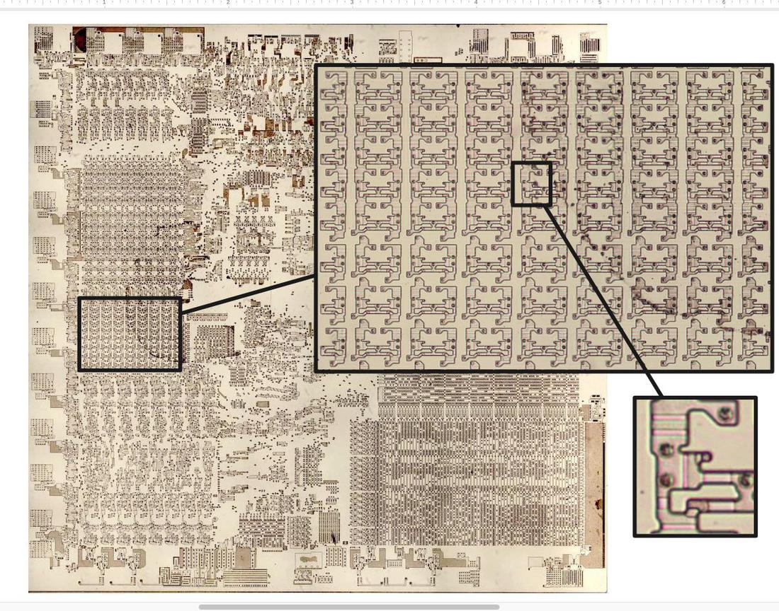
The photo below zooms in on the 8086's general-purpose register file, showing the matrix of register cells: 16 columns and 8 rows for eight 16-bit registers. It then zooms in on a single register cell in the register file. I'll now explain how this cell is implemented.

Die photo of the 8086, zooming in on the lower register file (eight 16-bit registers) and then a single register cell. The metal and polysilicon were removed for this photo to show the silicon structures.

Die photo of the 8086, zooming in on the lower register file (eight 16-bit registers) and then a single register cell. The metal and polysilicon were removed for this photo to show the silicon structures.

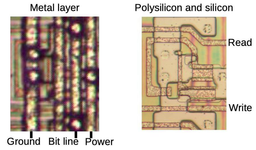
The 8086 is constructed from doped silicon and polysilicon wiring with metal wiring on top. The left photo below shows the vertical metal wiring of a register cell. The ground, power, and bit line wires are indicated. (The remaining wire crosses the register file but isn't connected to it.) In the right photo, the metal layer has been dissolved to show the polysilicon and silicon underneath. The read and write lines are horizontal polysilicon wires. (Because the chip has only one layer of metal, the register uses metal for the vertical lines and polysilicon for the horizontal lines so they don't run into each other.) The connections (called vias) between the metal and the silicon are visible as brighter circles in the metal photo and as circular spots in the silicon photo.

A register storage cell. The photo on the left shows the metal layer, while the photo on the right
shows the corresponding polysilicon and silicon underneath. The bright circles on the metal layer are vias connected to the circles on the silicon.

A register storage cell. The photo on the left shows the metal layer, while the photo on the right shows the corresponding polysilicon and silicon underneath. The bright circles on the metal layer are vias connected to the circles on the silicon.

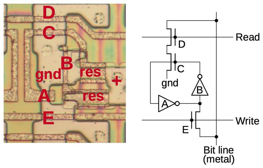
The diagram below shows how the physical layout of the register cell matches up with the schematic. The inverters are formed from transistors A and B, along with the resistors. Transistors C, D, and E are formed by the labeled strips of polysilicon. The bit line is not visible below, since it is in the metal layer. Note that the layout of the memory cell is highly optimized to minimize its size. Also note that transistor A is much smaller than the other transistors; inverter A has a weak output so it can be overpowered by the bit line when a value is written.

A register cell in the 8086 with the corresponding schematic.

A register cell in the 8086 with the corresponding schematic.

8-bit register support

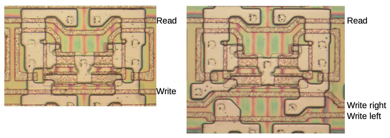
Careful examination of the die shows that some of the register cells have a slightly different structure. On the left is a pair of the register cells discussed above,5 while the right photo shows a pair of register cells with two write control lines instead of one. In the left photo, the write line crosses the silicon in both register cells. However, in the right photo, the "write right" line crosses the silicon on the right side but goes between the silicon regions on the left. Conversely, the "write left" line crosses the silicon on the left side and goes between the silicon on the right. Thus, one write line controls writes to the right-hand bit, while the other controls writes to the left-hand bit. In the full 16-bit register, this allows alternating 8-bit parts to be written separately.6

Two pairs of memory cells, showing different circuitry. The left cells have a single write line, while the right cells have separate write lines for the left and right bits.

Two pairs of memory cells, showing different circuitry. The left cells have a single write line, while the right cells have separate write lines for the left and right bits.

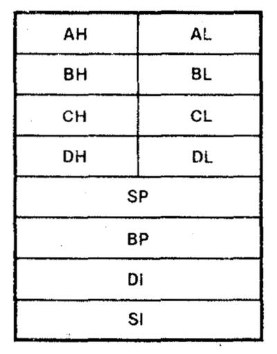
Why do some registers have two write lines while others have one? The reason is that the 8086 has 16-bit registers, but four of them can also be accessed as 8-bit registers, as shown below. For example, the 16-bit accumulator A can be accessed as an 8-bit AH (accumulator high) register and an 8-bit AL (accumulator low) register. By implementing the registers with two write control lines, either half of the register can be written separately.7

The general-purpose registers in the 8086 processor. The A, B, C, and D registers can be split into two 8-bit registers. From The 8086 Family User's Manual.

The general-purpose registers in the 8086 processor. The A, B, C, and D registers can be split into two 8-bit registers. From The 8086 Family User's Manual.

Multi-port registers

So far, I've discussed the eight general-purpose "lower registers". The 8086 also has seven "upper registers" used for memory accesses, including the infamous segment registers.8 These registers have a more complex "multi-port" design, allowing multiple reads and writes to take place simultaneously.9 For instance, the multi-ported register file would allow the program counter to be read, a segment register to be read, and a different segment register to be written, all at the same time.

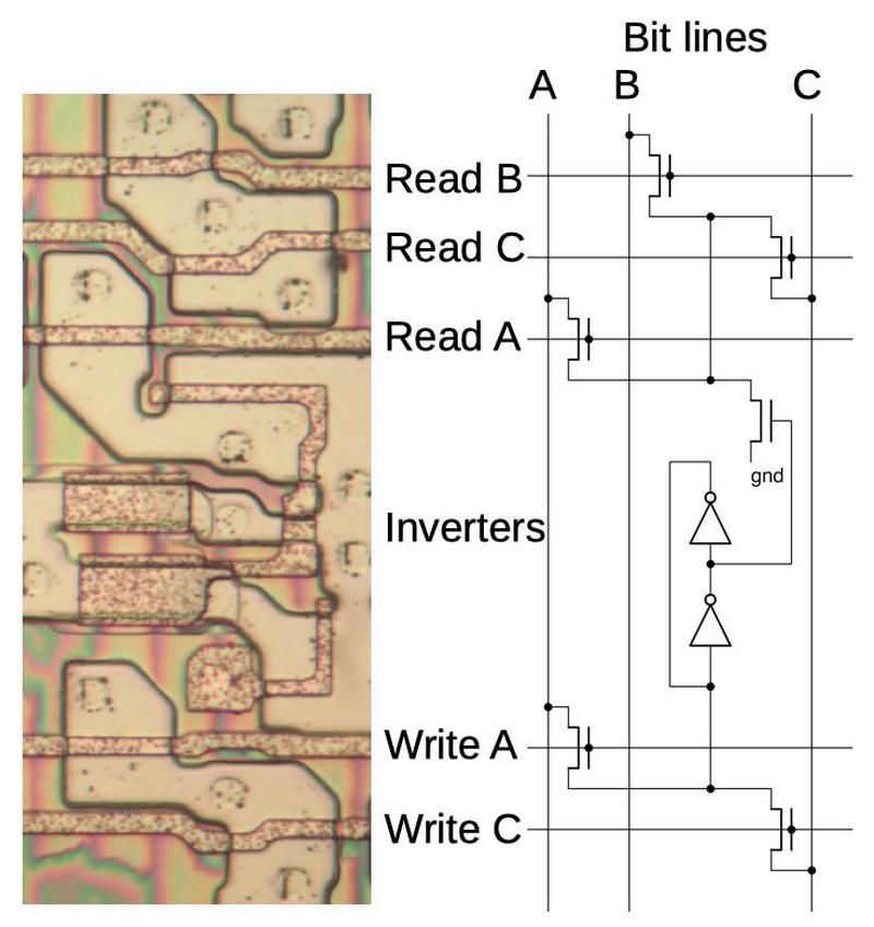
The multi-ported register cell below is built around the same two-inverter circuit as before but it has three bit lines (compared to one earlier) and five control lines (compared to two). The three read control lines allow the register cell contents to be read to any of the three bit lines, while the two write control lines allow bit line A or bit line C to be written to the register cell.

A multi-ported register cell in the 8086 processor.

A multi-ported register cell in the 8086 processor.

At first glance, the 8086's register file looked like a uniform set of registers, but close examination reveals that each register has been optimized based on its function.10 Some registers are simple 16-bit registers, which have the most compact layout. Other 16-bit registers can also be accessed as two 8-bit registers, requiring another control line. The most complex registers have two or three read ports and one or two write ports. In each case, the physical layout of the register cell has been carefully designed to be as compact as possible, with elaborate transistor shapes, as seen below. Intel's engineers shrunk the register layout as much as possible to fit all the registers in the available space.

The upper register file, consisting of ten 16-bit registers. This photo shows the silicon and polysilicon. The vertical red lines are traces of the metal layer that was removed. Click for a larger image.

The upper register file, consisting of ten 16-bit registers. This photo shows the silicon and polysilicon. The vertical red lines are traces of the metal layer that was removed. Click for a larger image.

Conclusions

Although the 8086 processor is 42 years old, it still heavily influences modern computing through the x86 architecture in heavy use today. The registers of the 8086 still exist in modern x86 computers, although the registers are now 64 bits long and have been joined by many new registers.

The 8086 is an interesting subject for die analysis since its transistors are large enough to be visible under a microscope. It was a complex processor at the time, with 29,000 transistors, but it is still simple enough that the circuitry can be traced out and understood. I plan to analyze the 8086 in more detail in future blog posts so follow me on Twitter @kenshirriff or on RSS for updates.11

Notes and references

  1. The 8086 was apparently the first microprocessor to implement instruction prefetching. The Motorola 68000 (1979) had a 4-byte instruction prefetch buffer. Prefetching in mainframes goes back to the IBM Stretch (1961), CDC 6600 (1964), and IBM System/360 Model 91 (1966). 

  2. It's difficult to determine how many registers are in a modern processor; the only accurate description I could find was in The Anatomy of a High-Performance Microprocessor, which describes the AMD K6 processor (1997) in detail. Due to register renaming modern processors have many more physical registers than architectural registers (the registers visible to a programmer), and the number of physical registers is not documented. (In addition to the eight general-purpose x86 registers, the K6 had 16 microarchitecture scratch registers for renaming.)

    Processors supporting AVX-512 include 32 512-bit registers, so that's 2 kilobytes of registers for that feature alone. This makes it even harder to determine the register size. As for cache size, high-end processors have up to 77 MB of cache storage.) 

  3. The pull-up resistor in an NMOS gate is actually a special transistor. The depletion-mode transistor acts as a resistor but is more compact and performs better than an actual resistor. 

  4. Other processors use slightly different register storage cells. The 6502 uses an additional transistor in the inverter feedback loop to break the feedback loop when writing a new value. The Z-80 writes to both inverters at the same time, making the transition "easier" but requiring two write wires. While the 8086 has an amplification transistor in each register cell for reads, other processors read the outputs from both inverters and use an external differential amplifier to strengthen the signal. The 8086's basic register cell uses 7 transistors (7T), more than a typical 6-transistor (6T) or 4-transistor (4T) static RAM cell, but it only uses one bit line rather than two differential bit lines. Dynamic memory (DRAM) is much more efficient, using one transistor and a capacitor, but data will be lost without refresh. 

  5. On the die, register cells are not repeated uniformly, but instead alternating cells are mirror images. This improves the density of the register cells because a power line running between two mirror-image cells can feed both of them (and the same with ground). Thus, the mirror-image layout reduces the number of power and ground lines by half. 

  6. Although block diagrams always show the 16-bit registers split into a left half and a right half, the actual implementation alternates the bits from each half instead of storing one 8-bit part on the left and the other on the right. This implementation makes it easier to swap the two halves of a 16-bit word, which is required in several cases. (One is an unaligned memory read or write. Another is an ALU operation using the top half of a register, such as AH.) Swapping bits between the left half and the right half would require running long wires between the halves for each bit. But with the interleaved implementation, swapping the two halves is a matter of swapping each pair of neighboring bits, which doesn't need long wires. In other words, the interleaved layout in the 8086's registers simplifies the wiring for swapping the two halves of a word. 

  7. If the register file only supported 16-bit registers instead of 8-bit half-registers, the processor could still work but would be less efficient. Writes to an 8-bit half could be done by reading the full 16 bits, modifying the 8-bit half, and then writing back the full 16 bits. This would take three registers accesses instead of one. Note that the register file doesn't need special support for 8-bit reads since the unwanted half can be ignored. 

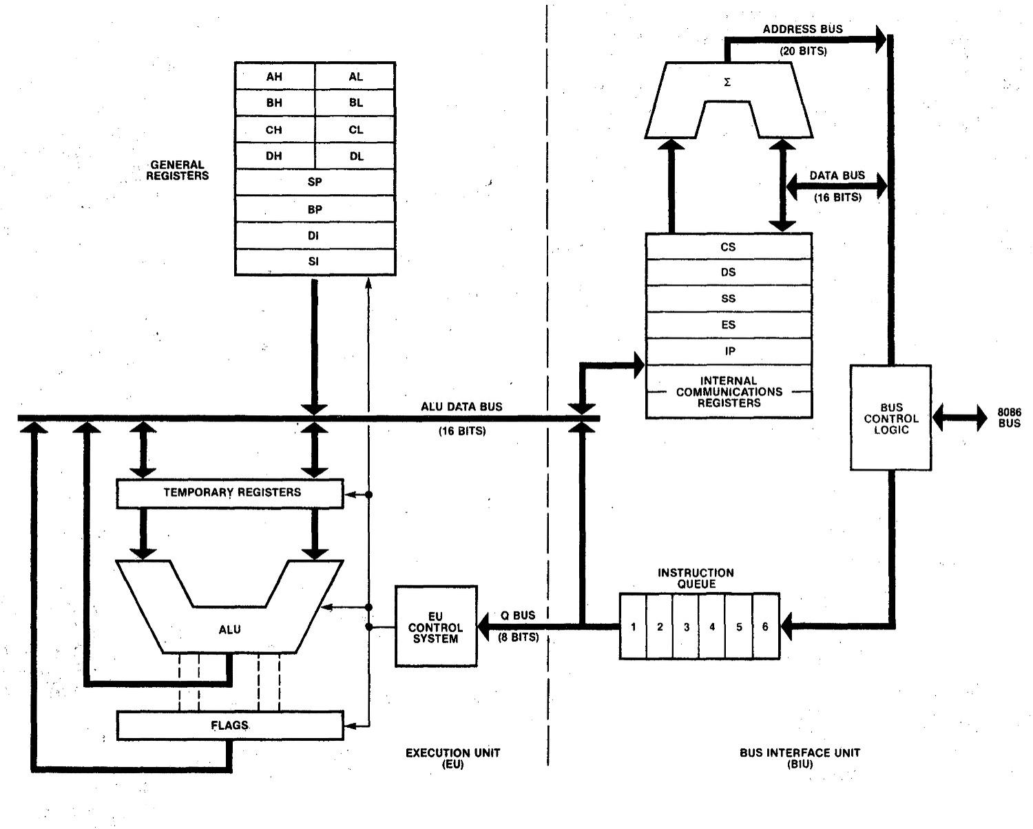
  8. The block diagram below is different from most 8086 block diagrams because it shows the actual physical implementation, rather than the programmer's view of the processor. In particular, this diagram shows two "Internal Communication Registers" in the Bus Interface Unit registers (right) along with the segment registers, matching the 7 registers visible on the die. (The temporary registers below are physically part of the ALU, so I'm not discussing them in this blog post.)

    Block diagram of the 8086 processor. From The 8086 Family User's Manual.

    Block diagram of the 8086 processor. From The 8086 Family User's Manual.


  9. The book Modern Processor Design discusses the complex register systems of processors from the early 2000s. It says that circuit complexity increases rapidly beyond 3 ports, but some high-end processors had register files with 20 ports or more.  

  10. The upper registers have differing numbers of read and write ports, as follows: two registers with 3 read control lines and 2 write lines, one register with 2 read lines and 2 write lines, and four registers with 2 read lines and 1 write line. The first three registers are probably the program counter, the "indirect" temporary register, and the "operand" temporary register. The last four are probably the SS, DS, SS, and ES segment registers. There are also three instruction prefetch buffer registers, each with 1 read line and 1 write line.

    The 8088 processor, used in the original IBM PC was essentially identical to the 8086, except it had an external 8-bit bus instead of a 16-bit bus to reduce system cost. The 8088's prefetch buffer was four bytes instead of six, presumably because four bytes was sufficient with the 8088's slower memory bus.

    Unlike the 8086, the prefetch registers in the 8088 support writing to 8-bit halves independently (similar to the 8088's A, B, C, and D registers, but with a different register cell design). The reason is the 8088 fetched instructions one byte at a time instead of one word at a time, due to its narrower bus. Thus, the 8088's prefetch registers need to support byte-sized writes, while the 8086 does word-sized prefetches. 

  11. I wrote about the 8086 die and the die shrink process earlier. For more about register files, see my posts on registers in the Z-80 and in the 8085