The Nintendo Game Boy contains an audio amplifier chip for sound through a speaker or headphones. In this post, I reverse-engineer this chip and compare it with the later Game Boy Color chip (reverse-engineered earlier). Unexpectedly the Game Boy Color uses an entirely different amplifier design from the original Game Boy, which may explain why the two systems sound different.
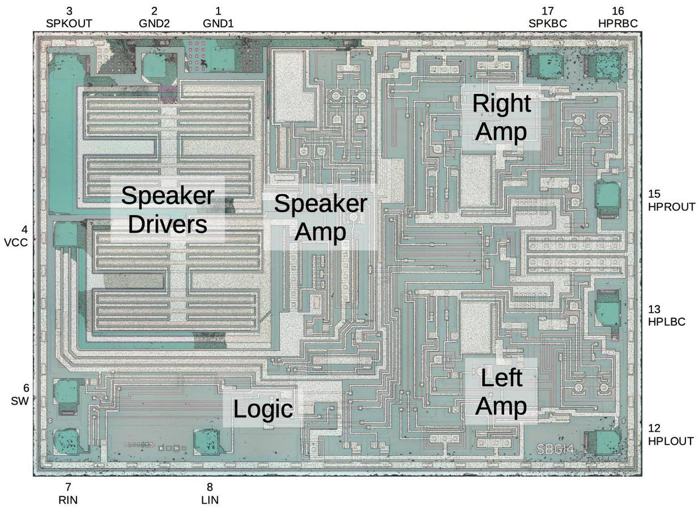
The diagram below shows the Game Boy amplifier's silicon die, with the main functional components labeled.1 The upper-left part of the chip has the two large driver transistors for the speaker output (one to pull the signal low and the other to pull the signal high). The headphone amplifier consists of two nearly-identical blocks: one for the left channel and one for the right. The circuitry for the current sources and current mirrors is shared by both headphone channels. The lower-left of the chip contains digital logic to enable either the speaker amp or the headphone amp, switching when the headphones are plugged in.
By examining the die closely, components such as transistors and resistors can be identified. From this, the complete circuit can be determined. In the photo above, the white lines are the chip's metal layer, connecting the components. The silicon itself appears greenish and is underneath the metal. The green squares around the outside are the pads where tiny bond wires connected the silicon die to the chip's 18 pins. Regions of the chip are treated (doped) to change the electrical properties of the silicon. The next sections explain how components are created from these different types of silicon.
NPN transistors
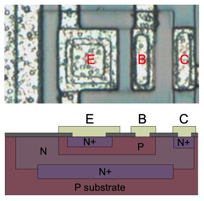
The amplifier chip is built from transistors known as NPN and PNP bipolar transistors, different from the low-power MOS transistors used in processors. These transistors have three connections: the emitter, the base, and the collector. The magnified photo below shows an NPN transistor from above. The slightly different tints in the silicon indicate regions that have been doped to form N and P regions, with dark lines separating the regions. The bubbly silverish areas are the metal layer of the chip on top of the silicon—these form the wires connected to the emitter, base, and collector.
Underneath the photo is a vertical cross-section illustrating how the transistor is constructed. The emitter (E) wire is connected to N+ silicon. Below that is a P layer connected to the base contact (B). And below that is an N+ layer connected (indirectly) to the collector (C). If you look at the vertical cross-section below the 'E', you can find the N-P-N layers that form the transistor.
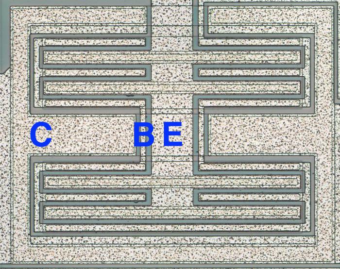
A different structure (below) is used for the high-current output transistors that drive the speaker. These transistors are much larger and have multiple interlocking "fingers" of the emitter and base, surrounded by the large collector. If you look back at the die photo, you can see two of these transistors filling the upper left part of the die.
PNP transistors
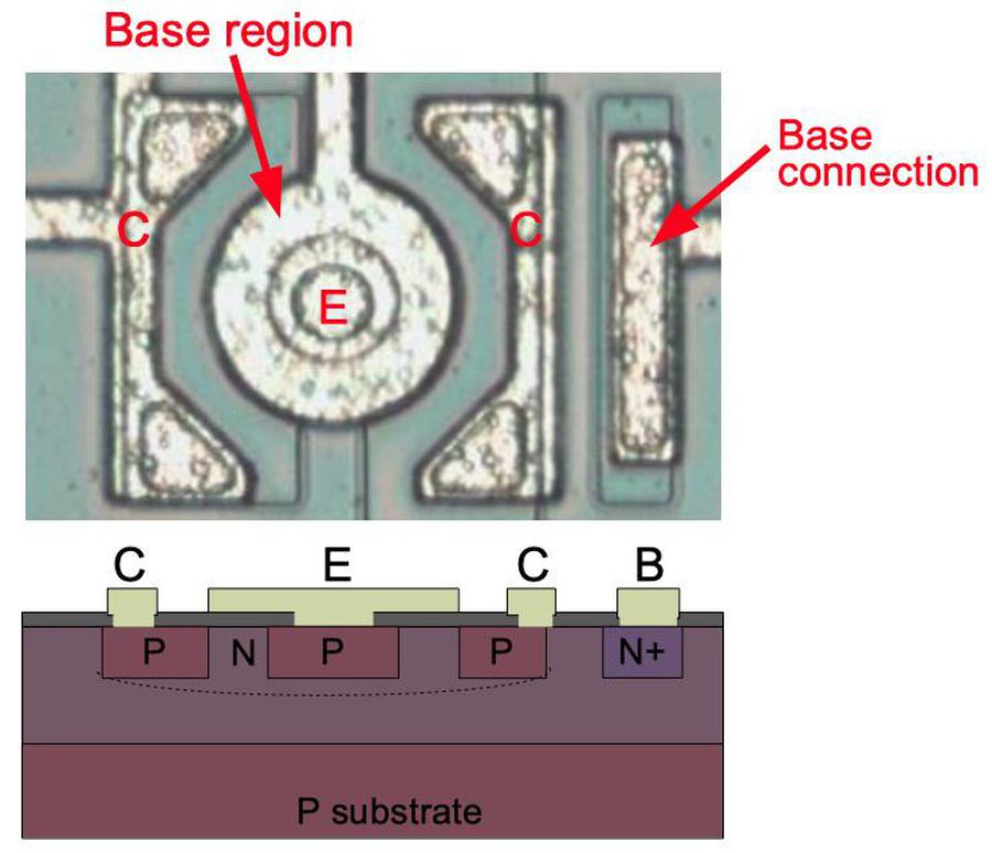
The chip also uses PNP transistors, which have an entirely different construction, as shown in the diagram below. The most obvious difference is that the PNP transistors are round.2 A PNP transistor has a small circular emitter (P-silicon), surrounded by a ring-shaped base region (N-silicon), which in turn is surrounded by the collector (P-silicon). (The emitter metal covers both the emitter and the base, but is only connected to the emitter.) These regions form a P-N-P sandwich horizontally (laterally), unlike the vertical structure of the NPN transistors. Note that although the base region physically surrounds the emitter, the metal connection to the base is further away; the base signal passes through the N region underneath the collector to reach the base region.
Resistors
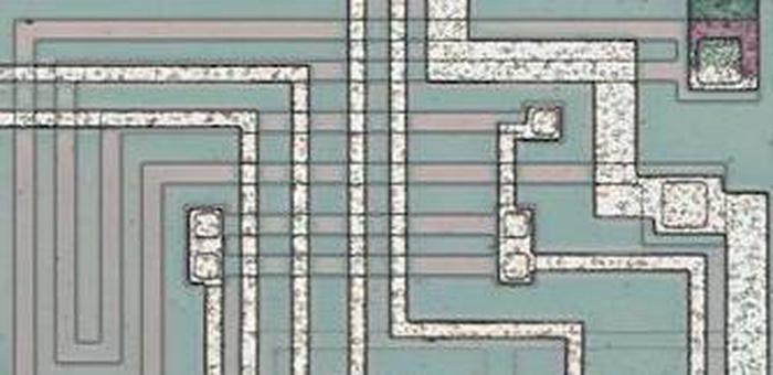
Resistors are an important component of analog chips. The photo below shows some long, zig-zagging resistors, formed from strips of P silicon, which appears beige in the photo. Its resistance is proportional to the length of the resistor, so large-value resistors have a zig-zag shape to fit in the available space. Because resistors are relatively large and inaccurate, chip designs try to minimize the number of resistors required. Even so, an analog chip like this one requires numerous resistors.
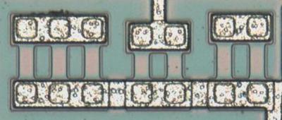
The photo below shows seven small resistors, but only the two in the middle are connected (in parallel) to the circuit. These extra resistors allow the resistance to be modified by modifying the metal layer, which is much easier than changing the silicon. (These resistors bias the output transistor, and it appears this is a critical resistance that required adjustment.)
Capacitors
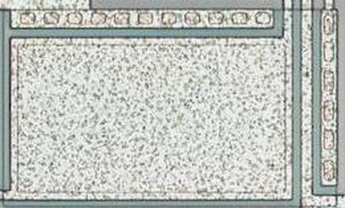
This chip has three large capacitors, one for each amplifier. The photo below shows one of the capacitors. The capacitors are simply a large layer of metal over the underlying silicon, separated by a thin insulating oxide layer. At the top and right of the photo, you can see the connections between the metal wiring and the underlying silicon. In this chip, capacitors are used to ensure the stability of the amplifiers. Because they are large, the three capacitors are easy to spot in the chip die photo.
The LM380
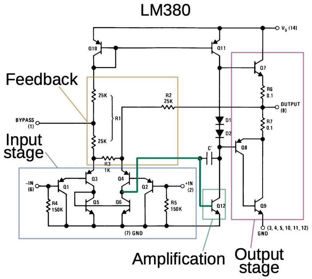
The Game Boy amplifier chip has a design very similar to the popular LM380 power audio amplifier chip (1972), so I'll start with an overview of how the LM380 works. (See the footnote5 for details.) The LM380 has positive and negative inputs and an output that amplifies the difference between the inputs by a fixed factor of 50. This may sound like an op-amp, but the LM380 is intended as an audio amplifier and is different from an op-amp in several ways: it has a small, fixed gain, it doesn't have a negative power supply, and its internal implementation is different.
The schematic below shows the main functional blocks of the LM380. The inputs go into a differential pair circuit (blue)3. The output from the differential pair (green) goes into a single-transistor amplification stage that provides more gain. The capacitor across the amplification stage stabilizes the amplifier to prevent oscillation. Finally, the output stage (purple) produces the high-current output: power transistor Q7 pulls the output high, while Q8 and Q94 pull the output low. The feedback network controls the gain of the LM380, fixing the gain at a factor of 50. Note that unlike an op-amp, the LM380's feedback network is connected to internal points of the amplifier, not the inputs.
Game Boy Audio chip: headphone amplifier
The Game Boy amplifier chip contains three amplifiers: two identical amplifiers for the left and right headphone channels, and a more powerful mono amplifier for the speaker. The Game Boy headphone amplifiers and the speaker amplifier are somewhat different, but they are both similar to the LM380.
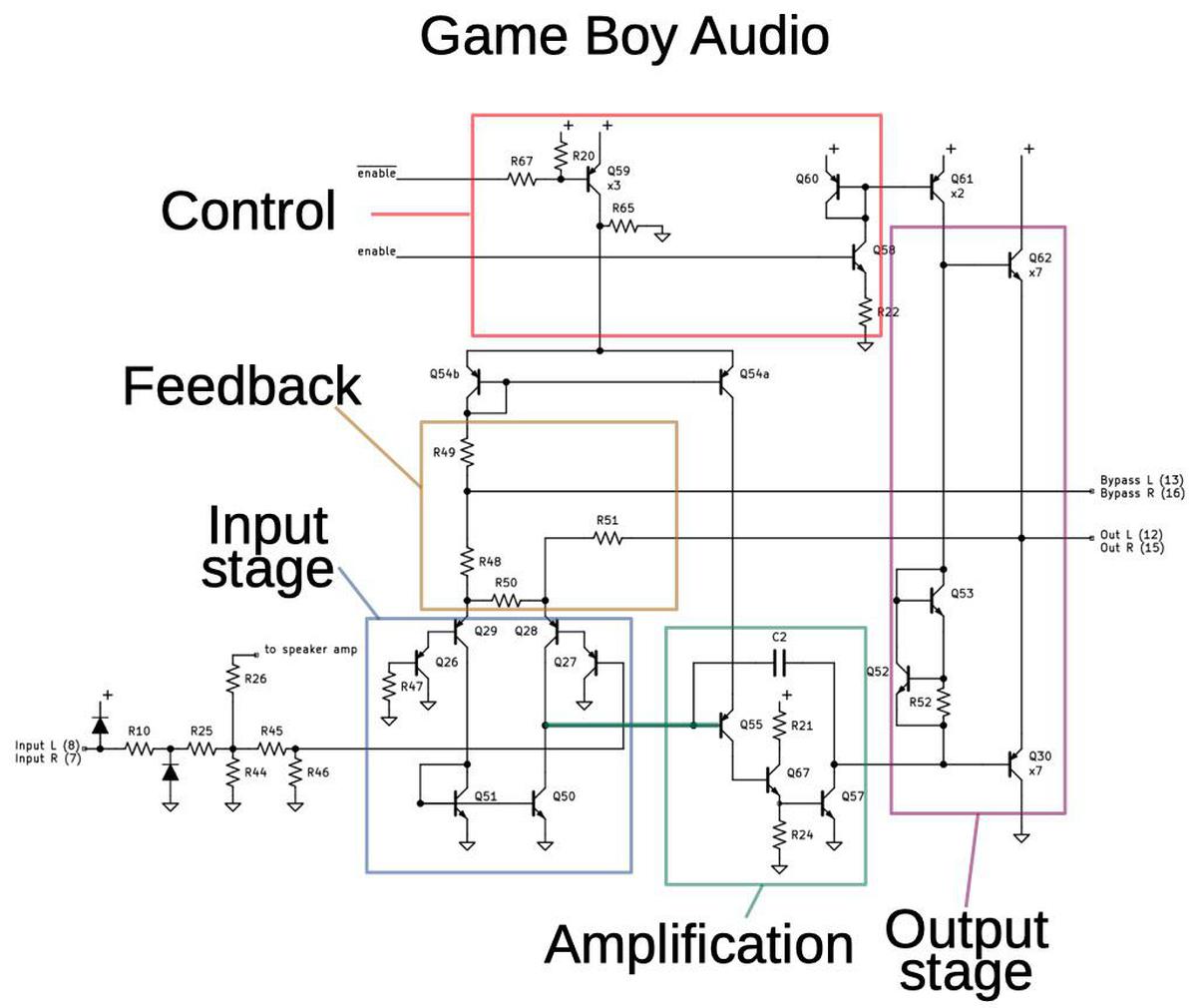
The schematic below shows the Game Boy headphone amplifier. Comparing it with the LM380 schematic above shows the similarities between the LM380 and the headphone amplifier, but also some differences. The input stage and feedback circuit of the LM380 are the most distinctive parts of that chip, and the headphone amplifier's circuit is essentially identical.6 The "Amplification" stage of the headphone amplifier has three transistors compared to one in the LM380, probably to produce more gain. The headphone amplifier's output stage is similar but simplified; the PNP/NPN pair that pulls the LM380 output low is replaced with a single PNP transistor. The biggest difference is the "Control" section of the headphone amplifier, which is not present in the LM380. This control circuitry powers down the headphone amplifier if headphones are not plugged in, conserving battery life.
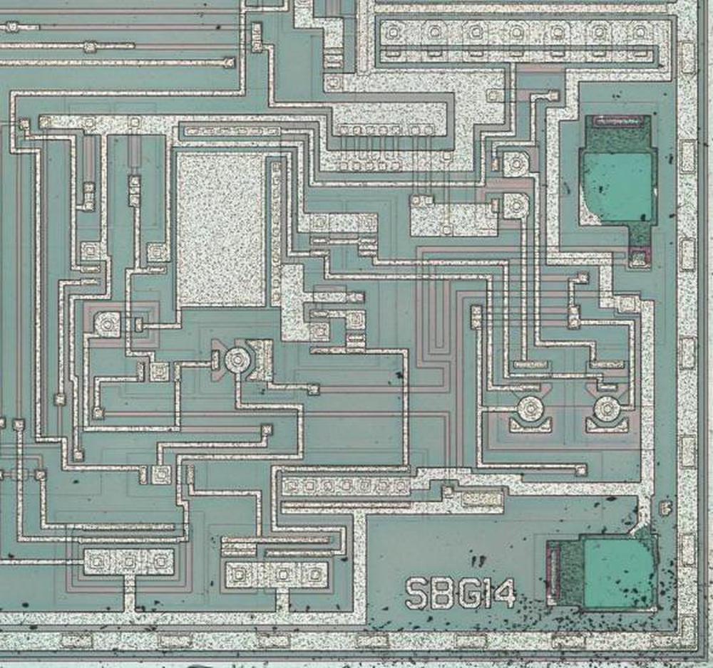
The photo below shows the left headphone amplifier. The output pin (lower-right, next to the part number SBG14) is driven by seven PNP transistors in parallel (top-left) and seven smaller NPN transistors in parallel (lower center). The capacitor is in the upper left, near the center. Many resistors snake around the die.
Game Boy Audio chip: speaker amplifier
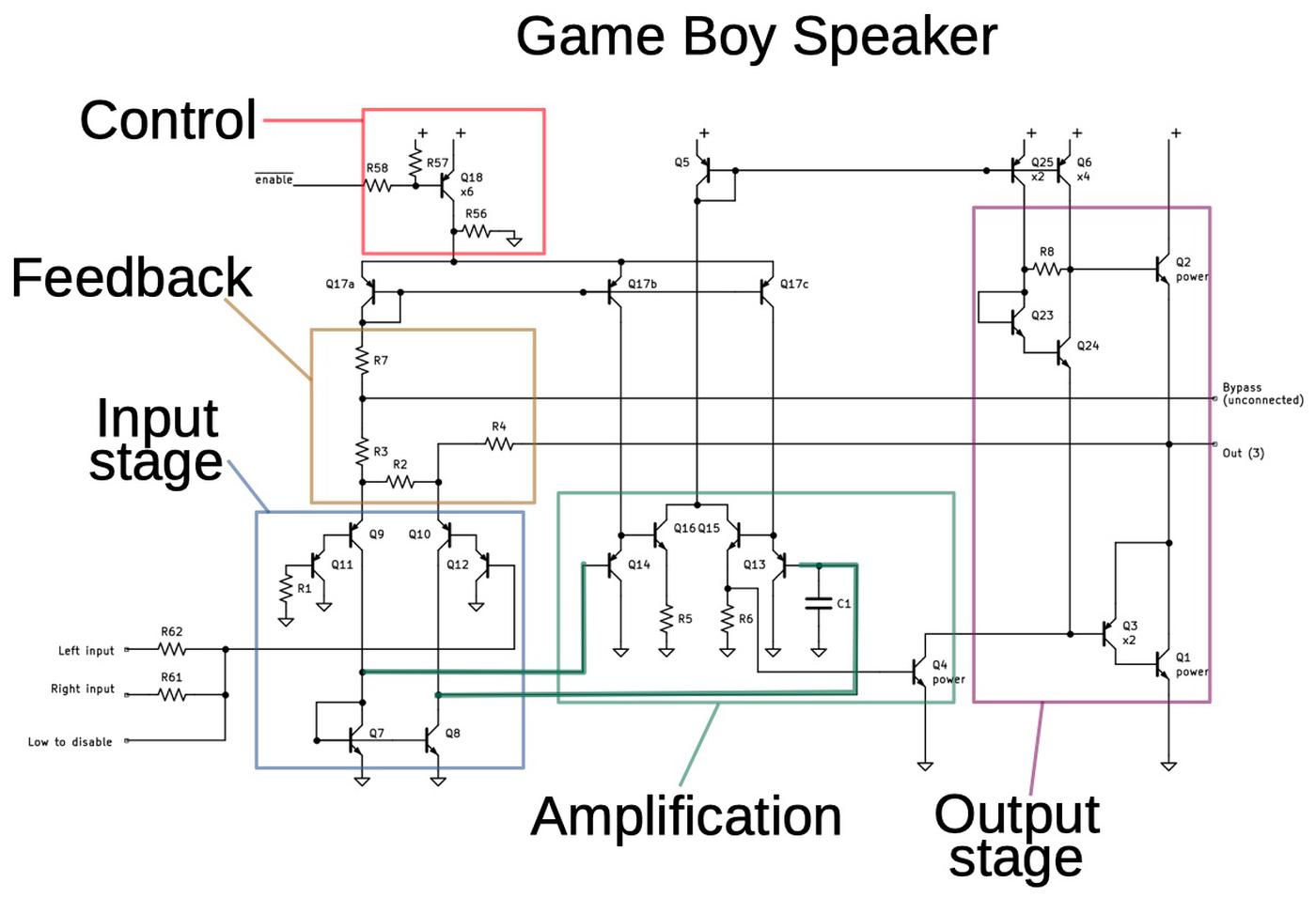
The next schematic shows the Game Boy speaker amplifier. Unlike the two channels for headphone amplification, there is a single speaker amplifier, producing a mixture of the left and right channels. Again, the input stage and feedback are almost identical to the LM380. The output stage has only minor differences. However, the amplification stage for the speaker is completely different: it includes a four-transistor differential amplifier stage, which will provide much more amplification.7 Although this amplification stage looks very similar to the input stage at first glance, its is wired differently and uses NPN transistors.8
The chip provides pins for bypass capacitors to reduce the effect of power supply fluctuations.9 The headphone amplifiers have external bypass capacitors, but the speaker bypass capacitor is omitted for some reason (see the Game Boy schematic). Lack of this capacitor may contribute to the background hum that people hear in the Game Boy's sound.
Comparison with the Game Boy Color
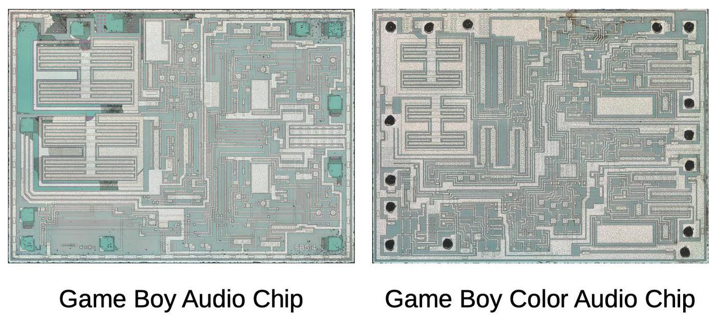
I recently reverse-engineered the Game Boy Color's amplifier chip, so it's interesting to compare the two chips. The amplifier chips for the Game Boy and the Game Boy Color provide similar functions. Even at the die level (below), the two chips look similar. They both have power transistors in the upper-left for the speaker, control circuitry in the lower-left, and two headphone channels on the right.
Surprisingly, the implementations of the two chips are completely different. While the Game Boy uses LM380-style audio amplifiers, the Game Boy Color uses power op-amps with more complicated circuitry. The most important difference is that the Game Boy chip has internal feedback to control the gain, while the Game Boy Color also has an external feedback capacitor, which causes it to act as a high-pass filter. For more information, see my Game Boy Color amplifier article and schematic.
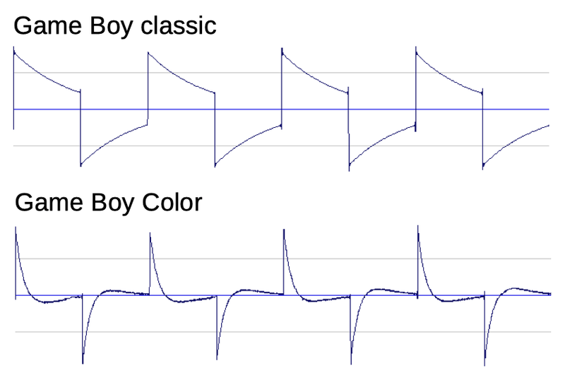
Collectors of Game Boy systems have noticed that the different versions have a very different sound (discussion). The original Game Boy has a "warm, bassy sound", while the Game Boy Color has a "thin sound" with background noise and hum. These aren't just subjective differences, but show up in the waveforms:
What's interesting is that we can explain much of the sound difference through the analysis of the amplifier chips. The Game Boy's output is close to a square wave, but the waveform drops somewhat due to the speaker's 100µF DC blocking capacitor (schematic). The amplifier in the Game Boy Color, on the other hand, is configured as a high-pass filter, so it outputs higher-frequency spikes, losing the bass sound.
Conclusion
The Game Boy (1989) and Game Boy Color (1998) use custom amplifier chips. By examining die photos, the circuitry can be reverse engineered. The chips are different from common amplifier chips in two main ways, which probably explains why custom chips were created. First, each chip has three amplifiers: two for headphone channels and one for the speaker. Second, to conserve power the chip has circuitry to power-down the unused amplifiers, based on whether or not headphones are plugged in. Reverse-engineering the chips also explains much of the difference in sound between the Game Boy and the Game Boy Color. The Game Boy Color's chip implements a high-pass filter, so the sound is thin and lacks the bass of the Game Boy.
I announce my latest blog posts on Twitter, so follow me @kenshirriff for future articles. I also have an RSS feed. My KiCad files for the schematic are on Github. Thanks to John McMaster for providing the chip photos; his page is here. Thanks to Herbert Weixelbaum for the sound waveforms.
Notes and references
-
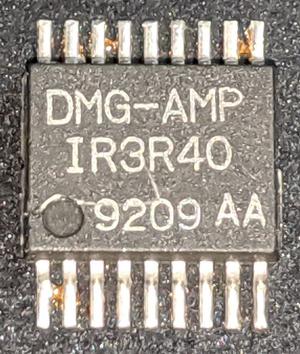
The audio amplifier chip is labeled DMG-AMP, standing for "Dot Matrix Game amplifier". The part number on this 18-pin chip (made by Sharp) is IR3R40.
The IR3R40 chip. Photo courtesy of John McMaster.Internally, the chip is labeled SBG14.
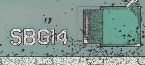
The die is labeled SBG14. -
Most of the PNP transistors on this chip are round. However, when multiple PNP transistors are combined, a square structure is used instead. The square PNP transistors are larger than the square NPN transistors. The chip also has some PNP transistors with multiple collectors. Other PNP transistors have no explicit collector connection but use the substrate (ground). ↩
-
The inputs to the LM380 (or Game Boy amplifier) go into a differential pair (Q3, Q4), but this differential pair is different from the standard one used in op-amps. In particular, the emitters receive different, varying currents, and this is where the feedback happens. ↩
-
The output stages of the LM380 and the Game Boy speaker amplifier use two transistors for pull-down configured as a Szilaki pair. The combined PNP and NPN transistors act as a higher-performance PNP transistor, somewhat like a Darlington pair. ↩
-
The LM380 is explained in detail in the National Semiconductor application note, and Power Audio Amplifier IC LM380. The similar LM386 is discussed in LM386 lecture and LM386 adventures.
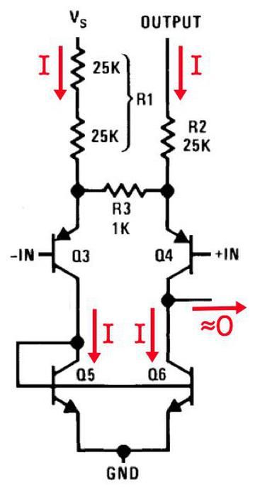
I'll explain the feedback network since the Game Boy chip operates the same way. The diagram below shows how the feedback network in the LM380 operates with no input. In the upper left, the supply voltage VS across R1 creates a current I. Transistors Q5 and Q6 form a current mirror: this forces the current through Q6 to match the current (I) through Q5. The current from Q4 to the rest of the chip must be approximately 0 (since it is strongly amplified by the rest of the chip). Putting this all together, the current through R2 (generated from the output voltage feedback) must also be I. Since R2 is half the resistance of R1, the output voltage must be half of the supply voltage. The conclusion is that the output voltage at idle will be half of the supply voltage, as desired.
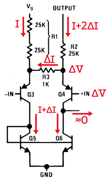
The LM380 with no signal applied. Schematic of the amplifier feedback network, from the LM380 datasheet.When inputs are applied, the feedback network acts as seen below. Suppose a voltage ΔV is applied to the positive input. Emitter-follower transistors Q3 and Q4 buffer and raise the inputs, so the same ΔV appears across resistor R3. This generates a current ΔI through the resistor. This increases the current through Q5 to I+ΔI, and because of the current mirror, the same current will flow through Q6. Adding up the various currents, the current through R2 must be I+2ΔI. Since R2 has 25 times the resistance of R3, 2ΔI corresponds to an increase in the output voltage of 50ΔV. Therefore, the input voltage is multiplied by a factor of 50. The point of this is that the feedback network fixes the gain at 50.
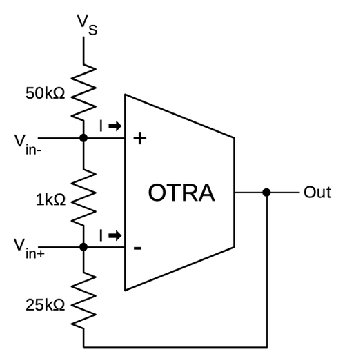
The LM380 with a small signal applied.It seems to me that the best way to understand the LM380 is to consider it as constructed from an operational transresistance amplifier (OTRA), an obscure relative of the op-amp. An OTRA acts like an op-amp, except the two inputs are currents instead of voltages, and the difference between the currents is amplified to produce the output voltage. The two currents (I) into the OTRA must be approximately equal, but the input voltages can diverge (unlike an op-amp).
My simplified schematic of the LM380, using an operational transresistance amplifier.The schematic above shows the LM380's circuitry represented as an operational transconductance amplifier and feedback network. Equating the two currents yields Vout = Vs/2 + 51V+ - 50.5V- or approximately Vout = Vs/2 + 50*(V+-V-). In other words, the output is centered at half the supply voltage, and the difference in input voltages is amplified by a factor of 50. (Nobody else describes the LM380 in this way, so it's quite possible that I am looking at it wrong, but this analysis makes sense to me.) ↩
-
I don't know the exact values of the resistances on the die, but by comparing lengths on the die I can determine ratios of resistances. Looking at resistors R48, R49, R50, and R51, I calculate that the speaker amplifier has a gain factor of 22. From resistors R2, R3, R4, and R7, I calculate that the speaker amplifier has a gain factor of 30, significantly more than the headphone amplifiers. ↩
-
Note that the overall amplification of the chip is limited by the feedback network. The idea of an op-amp is the raw gain will be something like 100,000, but the feedback reduces the gain to something reasonable like a factor of 50. The "extra" gain improves performance and reduces distortion. In other words, the additional amplification stage in the Game Boy compared to the LM380 isn't going to make it 100 times louder. ↩
-
I'm a bit puzzled by the second amplification stage for the speaker amplifier. It looks like a differential amplifier, except a differential amplifier normally has the emitters connected and this circuit has the collectors connected. ↩
-
The bypass capacitors used by the Game Boy chip (and the LM380) help reduce the impact of power supply fluctuations. It's common for chips to have a bypass capacitor between power and ground, but this bypass capacitor is a bit different. It is connected to a point in the feedback network where it is more effective than a regular bypass capacitor. ↩
My bipolar design skills are 20+ years rusty (I'm an integrated analog CMOS designer) but to me it looks like the collector-coupled NPN devices in the amplification stage of of the speaker amplifier look like some sort of absolute-value circuit. Looking at how the output stage is then biased from there, I think that this is intended to control the quiescent current (and crossover distortion) in the Class-AB output stage and keep the power dissipation under control. I suspect the designers found that in order to have acceptable crossover distortion for the speakers they needed to have higher quiescent current than in the headphone amplifiers, and if they had kept that current constant over the entire output voltage range they would have been over their power dissipation budget.
ReplyDeleteAnd yes, your explanation of the LM380 as an OTRA makes sense to me. Mind you, I've always been a fan of current-mode circuitry in general and current conveyors and translinear circuits in particular.
That was very thorough with a very interesting conclusion! Thanks!
ReplyDeleteThe collector connected circuit is a subtractor, out = ina -inb
ReplyDeleteBut ina = Out of the differential pair and inb = -Out
So the final output is 2xOut
Nonlinearities can be expected to be roughly equal on both sides of the differential pair, so this circuit subtracts them out.
Given the substantial die area devoted to the amplifiers, I'm surprised -- mainly for cost reasons, but also because of the similarly you note to existing audio-focused opamp designs -- that they didn't just use an off-the-shelf opamp and implement only the control circuitry as custom silicon. There appears to be room on the PCB for a few more components (opamp, resistors, caps), so that doesn't seem to be the issue.
ReplyDelete