The revolutionary Intel 8086 microprocessor was introduced 42 years ago this month so I've been studying its die.1 I came across two 8086 dies with different sizes, which reveal details of how a die shrink works. The concept of a die shrink is that as technology improved, a manufacturer could shrink the silicon die, reducing costs and improving performance. But there's more to it than simply scaling down the whole die. Although the internal circuitry can be directly scaled down,2 external-facing features can't shrink as easily. For instance, the bonding pads need a minimum size so wires can be attached, and the power-distribution traces must be large enough for the current. The result is that Intel scaled the interior of the 8086 without change, but the circuitry and pads around the edge of the chip were redesigned.
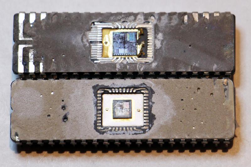
The photo below shows an 8086 chip from 1979, and a version with a visibly smaller die from 1986.3 (The ceramic lids have been removed to show the silicon dies inside.) In the updated 8086, the internal circuitry was scaled to about 64% of the original size by length, so it took 40% of the original area. The die as a whole wasn't reduced as much; it was about 54% of the original area. (The chip's package was unchanged, the 40-pin DIP package commonly used for microprocessors of that era.)
The 8086 is one of the most influential chips ever created; it started the x86 architecture that still dominates desktop and server computing today. Unlike modern CMOS processors, the 8086 was built from NMOS transistors, as were the 6502, Z-80, and other early processors.4 The first chip was built with HMOS,5, Intel's name for this process. Intel introduced improved HMOS-II in 1979 and in 1982, Intel moved to HMOS-III, the process used for the newer 8086 chip.6 Each newer HMOS version shrunk the size of features on the chip and improved performance.
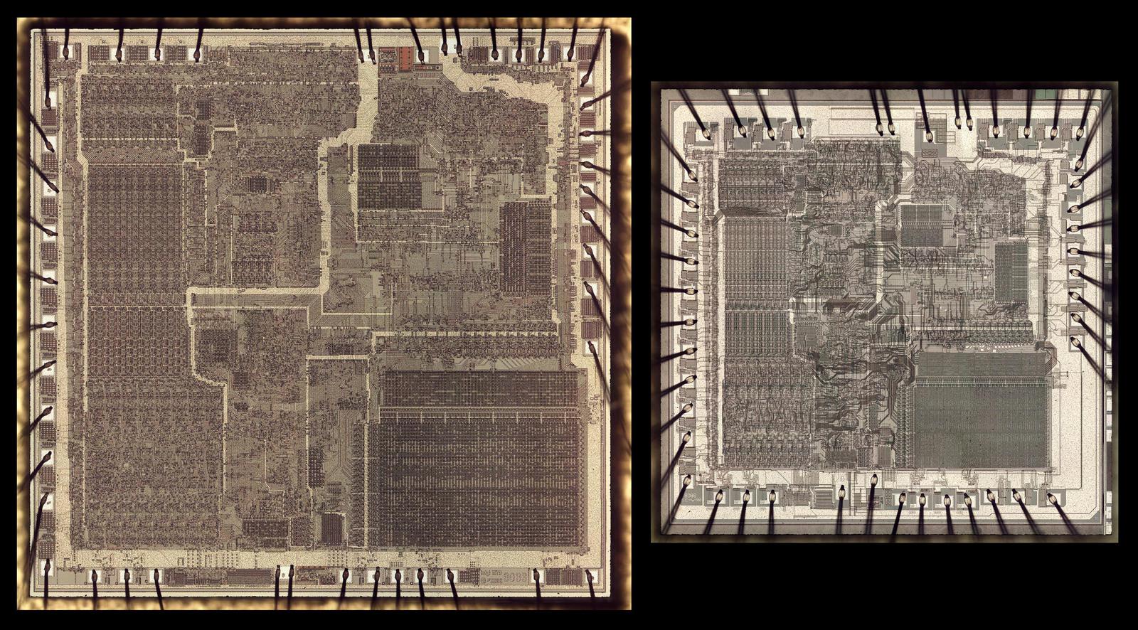
The photo above shows the two 8086 dies at the same scale. The two chips have identical layout in the interior,7 although they may look different at first. The chip on the right has many dark lines in the middle that don't appear on the left, but this is an artifact. These lines are the polysilicon layer, underneath the metal; the die on the left has the same wiring, but it is very faint. I think the newer chip has a thinner metal layer, making the polysilicon more visible.
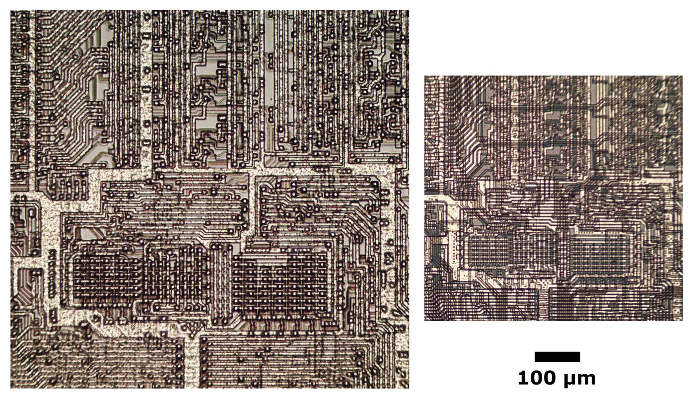
The magnified photo below shows the same circuitry on the two dies. There is an exact correspondence between components in the two images, showing the circuitry was reduced in size, not redesigned. (These photos show the metal layer on top of the chip; some polysilicon is visible in the right photo.)
However, there are significant differences around the edges of the dies. The bond pads around the outside are closer together, especially in the bottom right. There are two reasons for this. First, the bond pads can't shrink very much, since they need to be large enough to attach bond wires. Second, the power distribution traces around the edges are wider in order to support the necessary current. (Look to the right of the microcode ROM in the lower right, for instance.) Part of this is because the power traces in the middle of the circuitry were scaled down with the rest of the circuitry, so they are smaller; the outside traces need to pick up the slack. In addition, the thinner metal layer in the newer chip can't support as much current without being widened.
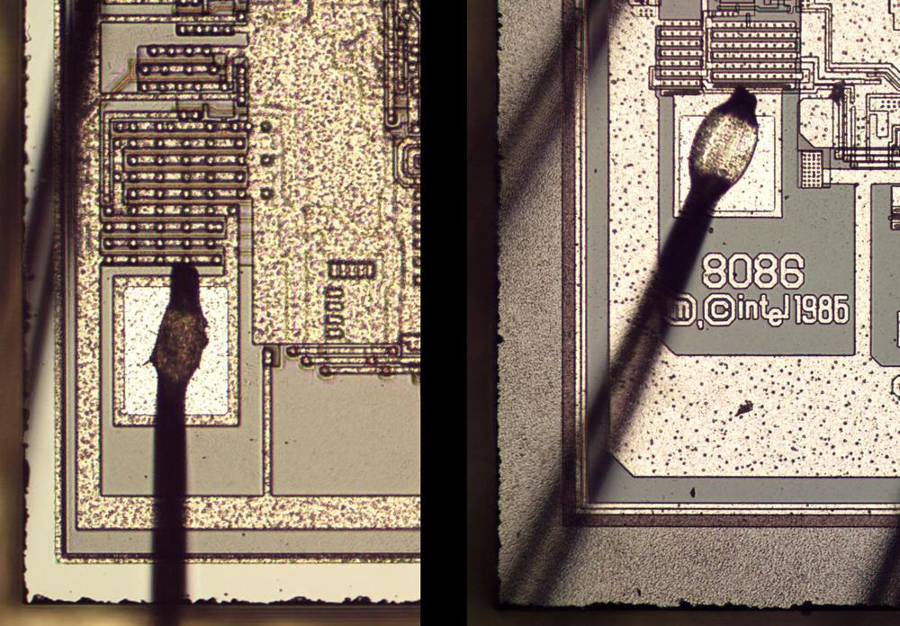
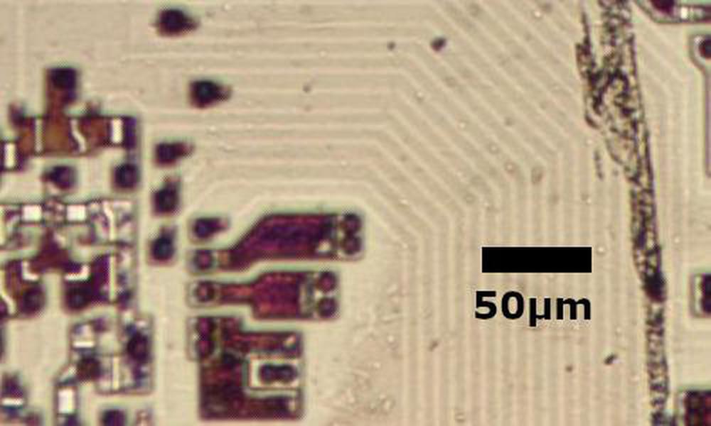
The photo above shows a bonding pad with an attached bond wire. The drive transistors are above the pad. The newer chip has almost the same size pad, but the power drive transistors have both shrunk and been redesigned. Note the much thicker metal power wiring on the newer chip. The Intel logo was moved from the bottom right to the bottom left, probably because that's where there was room.
A closer look at the dies
First, a bit of background on the NMOS construction used in the 8086 and other chips of that era. These chips consist of a silicon substrate, which is doped (diffusion) with arsenic or boron to form transistors. On top, a layer of polysilicon creates the gates of the transistors as well as providing wiring between components. Finally, a single metal layer on top wires up the components.
A semiconductor process (such as HMOS-III) has specific rules on the minimum size and spacing for features on the silicon, polysilicon, and metal layers. By looking closely at the chips, we can see how the features correspond to the design rules for HMOS I and HMOS III. The table below (from HMOS III Technology) summarizes the characteristics of the different HMOS processes. The features get smaller and the performance gets better with each version. (Intel got a 40% overall performance improvement going from HMOS-II to HMOS-III.)
| HMOS I | HMOS II | HMOS III | |
|---|---|---|---|
| Diffusion Pitch (µ) | 8.0 | 6.4 | 5.0 |
| Poly Pitch (µ) | 7.0 | 5.6 | 4.0 |
| Metal Pitch (µ) | 11.0 | 8.0 | 6.4 |
| Gate Oxide Thickness (Å) | 700 | 400 | 250 |
| Channel Length (µ) | 3.0 | 2.0 | 1.5 |
| Idsat (mA) | 8.0 | 14.0 | 27.0 |
| Minimum Gate-Delay (ps) | 1000 | 400 | 200 |
| Speed-Power Product (pJ) | 1.0 | 0.5 | 0.25 |
| Linear Shrink Factor | 1.0 | 0.8 | 0.64 |
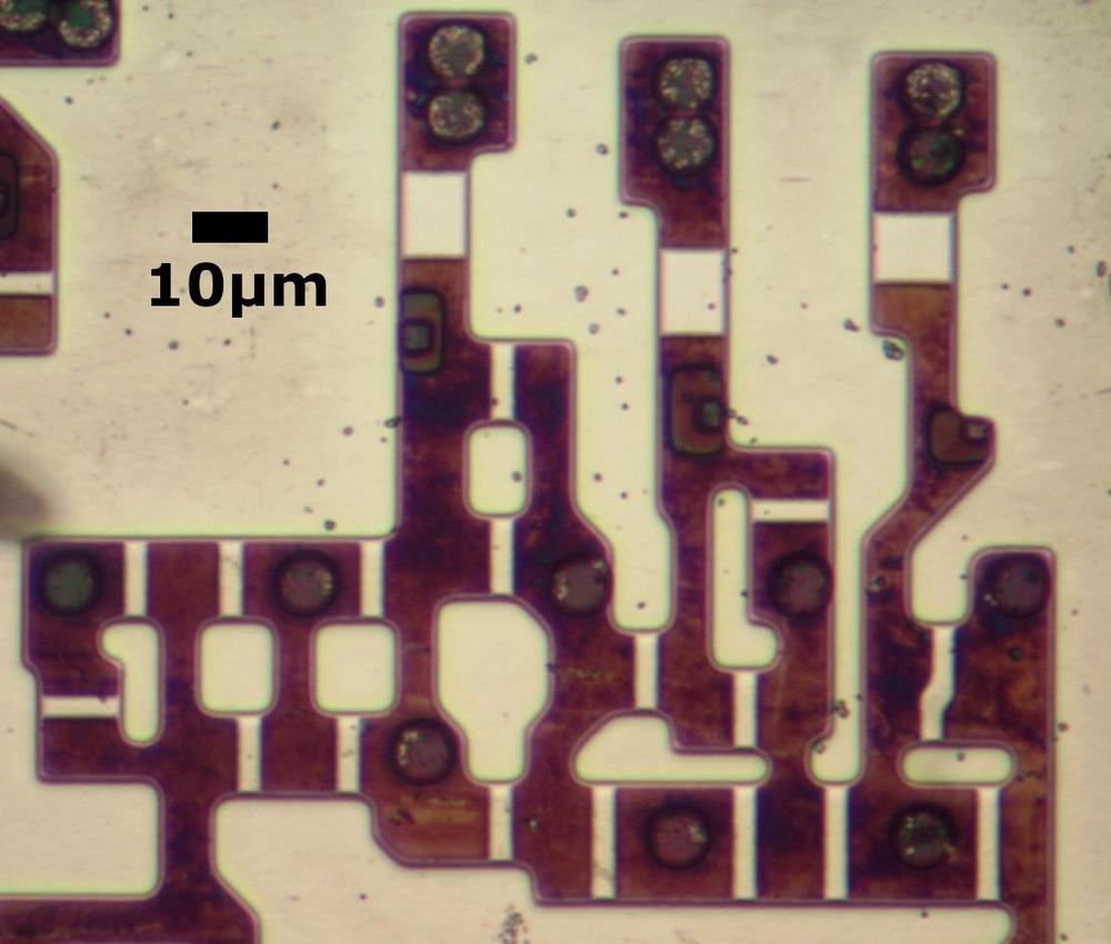
The microscope photo below shows a complex arrangement of transistors in the older 8086 chip. The dark regions are doped silicon, while the white rectangles are the transistor gates. (There are about 21 transistors in this photo.) A key measurement is the channel length, the length of the gate between the source and drain. (This is the narrower dimension of the white rectangles.) I measured 3 μm for these transistors, which nicely matches the published value for HMOS I.8 This indicates the chip was manufactured with a 3 μm process; in comparison, processors are now moving to a 5 nm process, 600 times smaller.
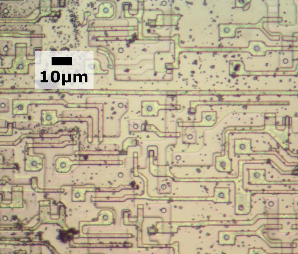
The photo below shows transistors in newer 8086 at the same scale; the transistors are much smaller. The linear dimensions are scaled by 64%, so the transistors have 40% of their original area. Because I processed this die differently, the polysilicon remained on the die, the yellowish lines. The doped silicon appears pinkish, much less visible than before. I measure the gate length as 1.9 μm, which is 64% of the previous 3 μm. Note that HMOS-III supports a considerably smaller 1.5 μm channel length, but since everything shrinks by the same 64% factor, the channel length is larger than necessary. This illustrates that uniformly shrinking the die wastes some of the potential gain from the new process, but it is much easier than completely redesigning the chip.
I also looked at the spacing (pitch) of lines in the metal layer. The photo below shows some horizontal and vertical metal wiring in the older chip. I measured 11μm pitch for the metal lines, which matches the published HMOS I figure. The shrink to 64% yields 7 μm pitch on the new chip, even though HMOS III supported 6.4 μm. As before, the constant shrink factor doesn't take full advantage of the new process.
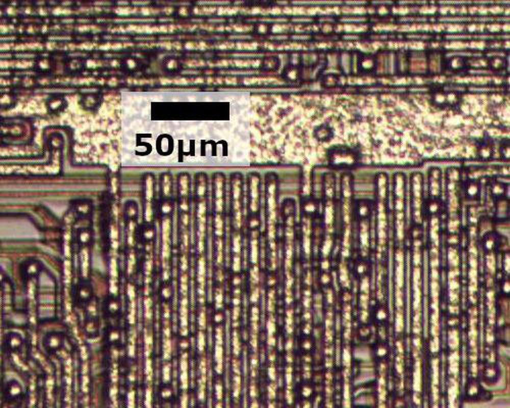
Finally, I looked at the pitch of the polysilicon wiring. The photo below shows the older 8086; the polysilicon has been removed leaving faint white traces. These parallel polysilicon lines probably formed a bus, routing signals from one part of the chip to another. I measured 7 μm pitch for the polysilicon lines, matching the published HMOS figure. (Interestingly, polysilicon wiring can be denser than metal wiring under HMOS rules.) The newer chip has 4.5 μm polysilicon pitch, compared to possible 4.0 μm.
Conclusions
A die shrink provides a way to improve the performance of a processor and reduce its cost without the effort of a complete redesign. Comparing the two chips, however, shows that a die shrink is more complex than uniformly shrinking the whole die. While most of the circuitry is a straightforward shrink, the bond pads didn't shrink to the same degree, so they needed to be moved around. The power distribution was also modified, adding more power wiring around the outer part of the chip.
Modern microprocessors still use die shrinks. In 2007, Intel moved to a tick-tock model, where they would alternate shrinks of an existing chip (the "tick") with the production of a new microarchitecture (the "tock").
I plan to analyze the 8086 in more detail in future blog posts so follow me on Twitter at @kenshirriff for updates. I also have an RSS feed.
Notes and references
-
The 8086 was released on June 8, 1978. ↩
-
It's actually quite remarkable that MOSFET circuits still work after being scaled down over a large range, since most things don't scale as easily. For instance, you can't scale down an engine by a factor of 10 and expect it to work. Most physical things suffer from the square-cube law: the area scales with the square of the ratio, while the volume scales with the cube of the ratio. For MOS circuits, however, most things either stay the same with scaling, or get better (such as frequency and power consumption). For more details on scaling, see Mead and Conway's Introduction to VLSI Systems Ch 1 sect 2. Interestingly, that 1978 book says that scaling had a fundamental limit of 1/4 micron (250 nm) channel length due to physical effects. That limit was wildly wrong; transistors are now moving to 5 nm, through technologies such as FinFETs. ↩
-
The older chip says ©'78, ©'79 on the package and ©1979 on the die and has a 7947 (47th week of 1979) date code on the underside. The newer chip says ©1978 on the package but ©1986 on the die and has no identifiable date code, so I figure it is from 1986 or slightly later. It's unclear why the newer chip has an older copyright date on the external package. ↩
-
A brief description of the technologies in early processors. N-channel MOSFETs are a particular type of MOSFET transistor. They have considerably better performance than the P-channel MOSFETs used in the earliest microprocessors, such as the Intel 4004. (Modern processors use N-channel and P-channel transistors together for lower power consumption; this is CMOS.) Gates built from N-channel MOSFETs require a pull-up resistor, which is implemented by a transistor. Depletion load transistors are a type of transistor introduced in the mid-1970s that perform better as pull-up resistors and don't require an extra power supply voltage. Finally, MOS transistors originally used metal for the gate (the M in MOS). But in the late 1960s, Fairchild developed the use of polysilicon for the gate instead of metal. This provided much better performance and was easier to manufacture. The point of all this is that between the late 1960s and mid-1970s, several radical changes were introduced in MOS integrated circuit production, and these led to the success of the 6502, Z-80, 8085, 8086, and other early processors. In the 1980s, CMOS processors took over due to their lower power consumption and better performance. ↩
-
Strangely, it's unclear what the "H" stands for in HMOS. I couldn't find anywhere that Intel expands the acronym; databooks refer to "Intel's advanced N-channel silicon gate HMOS process" or say "HMOS is a high-performance n-channel MOS process". Intel later defined CHMOS as Complementary High Speed Metal Oxide Semiconductor) (example). Motorola defined HMOS as High-density MOS (example) while other sources defined it as High-speed MOS or High-density, short channel MOS. Intel has a patent on "High density/high speed MOS process and device", so perhaps the "H" stands for both "high density" and "high speed". ↩
-
Interestingly, Intel used a 4K static RAM chip to develop each of their HMOS processes, before using the process for their microprocessors and other chips. They probably developed with the RAM chip because it has dense circuitry, but is relatively easy to design because it repeats the same memory cell over and over. Once they had all the design rules figured out, then they could create the much more complex processor. ↩
-
I scaled complete, high-resolution images of the two chips to compare and the main part of the chips is an exact match except for some trivial changes. I found a couple of places where a via was slightly moved, which is puzzling because I see no logical reason for that. The circuit was unchanged, so it's not a bug fix. One question is if there were any microcode changes. The microcode looks identical, but I didn't do a bit-by-bit comparison. ↩
-
You may have noticed that three transistors in the photo have much larger gates. These are transistors that are acting as pull-up resistors, as is typical for NMOS circuits. The larger size makes the transistors weaker, so they provide a weak pull-up current. ↩
Thanks for your work. I am reading pretty much each of your chip analysis blog posts.
ReplyDeleteYour historical analysis work is wonderful, informative and brings back many fond memories of developing with the Intel x86 chips.
ReplyDeletePlease consider adding a 'date written' field to your blog posts. While this can usually be inferred from your blog directory structure when saving a posting, I believe an embedded time stamp would aid future semiconductor historians that serendipitously come across a snapshot save of one of your blog postings.
The 8086 was a poor design compared to the 6800 and later 68000 true 32-bit processor. Intel's 8086 segmented memory model plagued software development for many years. Good journalism would have noted this :/
ReplyDeleteI do not agree to your last statement since the article deals with chip technology and not with architecture - although I agree to the statement itself.
DeleteBTW: I am a 6502/99xx(x) lover and a x86 hater...
@Ken: excellent article!
One of the early motivations for "silicon compilers" was to replace optical shrinking with generating the design again from the same sources but with new design rules. In theory this would avoid the waste you measured.
ReplyDeleteAs always, it's amazing how great your articles are. Only one question: does the newer CPU run faster than the original design? I mean in raw frequency, I suppose that on a clock by clock comparison they must be identical.
ReplyDeleteJose Miguel Castillo: yes, Intel doubled the clock frequency from 5 MHz to 10 MHz with the improved process.
ReplyDeleteFascinating as usual! Regarding your footnote 5, "Strangely, it's unclear what the "H" stands for in HMOS." I was just reading an old Intel marketing piece called "A Revolution in Progress, a History of Intel to Date", published in 1984:
ReplyDeletehttps://www.intel.com/Assets/PDF/General/15yrs.pdf
In it, they define HMOS on page 28 as follows:
"No sooner had the 2115 hit the field than Pashley's group was assigned the task of getting Intel into the high-performance MOS business. They experimented with a number of approaches, "some very elegant but for the most part difficult to build", explained Pashley. Finally they zeroed in on what was later called HMOS (high-performance MOS), which involved scaling the transistors and using positive photoresist and projection printing. In just six months the team characterized the process and used it to shrink the 2115 die to about half its previous size. This was the start of the shrink technology concept, which led to the design and manufacture of the 2147 static RAM, Intel's first HMOS product."
Thanks for the great article.
-Rob
Re footnote 5, I was at DEC when they were using HMOS in 1981 (a deal with Intel). H stands for high performance.
ReplyDeleteNote 6 states that Intel probably developed the HMOS process with the RAM chip because it has dense circuitry but is relatively easy to design. I think that another benefit is that RAM is also easy to test exhaustively and it also makes it relatively easy to diagnose a failure. In contrast, it's more difficult to test exhaustively a CPU or understand a failure's cause.
ReplyDelete