I saw an ad for a tiny chip1 that provides 5 volts2 of isolated power: You feed 5 volts in one side, and get 5 volts out the other side. What makes this remarkable is that the two sides can have up to 5000 volts between them. This chip contains a DC-DC converter and a tiny isolation transformer so there's no direct electrical connection from one side to the other. I was amazed that they could fit all this into a package smaller than your fingernail, so I decided to take a look inside.
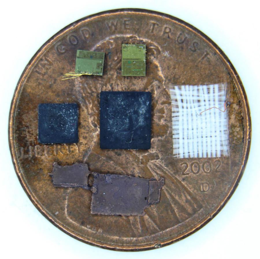
I obtained a sample chip from Texas Instruments. Robert Baruch of project5474 decapped this chip for me by boiling it in sulfuric acid at 210 °C. This dissolved the epoxy package, leaving a pile of tiny components, shown below with a penny for scale. At the top are two tiny silicon dies, one for the primary circuitry and one for the secondary. Below the dies are two magnetized ferrite plates from the transformer. To the right is one of five pieces of woven glass fiber. At the bottom is a copper heat sink, partially dissolved by the decapping process.3
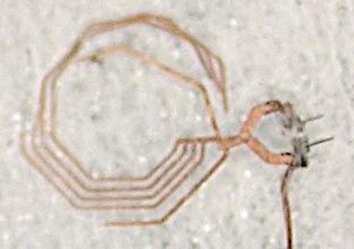
The chip also contained two octagonal copper coils that were the transformer windings. The photo below shows the remnants of one coil after decapping. These windings were probably copper traces on tiny printed circuit boards; the pieces of woven glass fiber are the remnants of these boards after the epoxy was dissolved. It appears that the winding consisted of multiple wires in parallel, rather than a coiled wire.
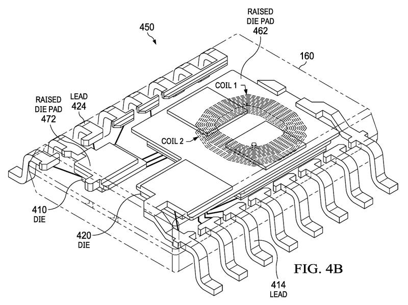
To determine how the components went together, I studied Texas Instruments patents and found a similar power isolation chip (below). Note the structure of the two dies and the coils. A key feature of this patent is the leads are raised internally, with the dies mounted upside down. This provides better electromagnetic isolation from the circuit board.
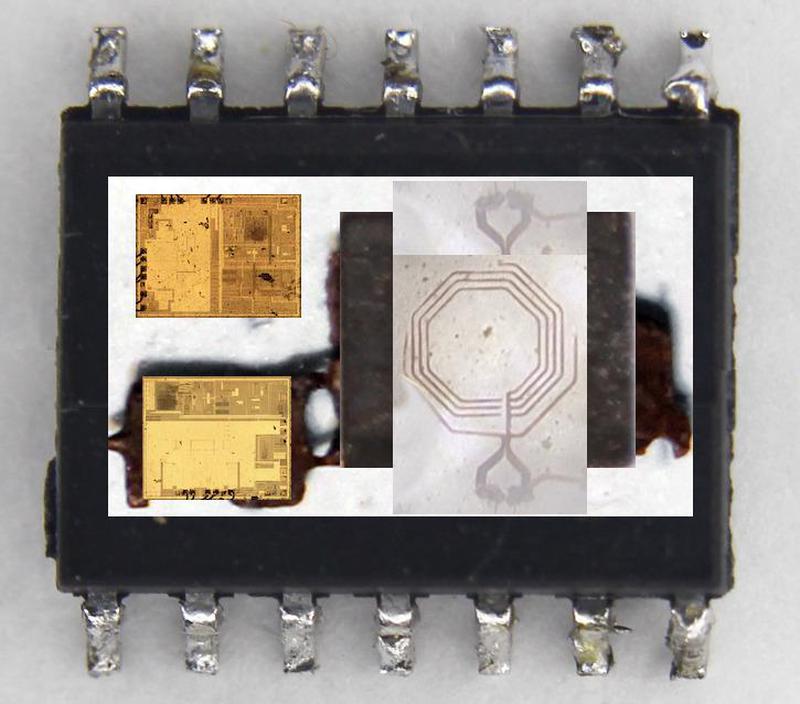
The chip is in a SOIC package, smaller than a fingernail. The mockup image below shows that the silicon dies and the transformer winding are so small that they can fit in this package.4 This power chip is about twice as thick as a standard SOIC package so it can hold the multiple layers of the transformer.`
The secondary die and its components
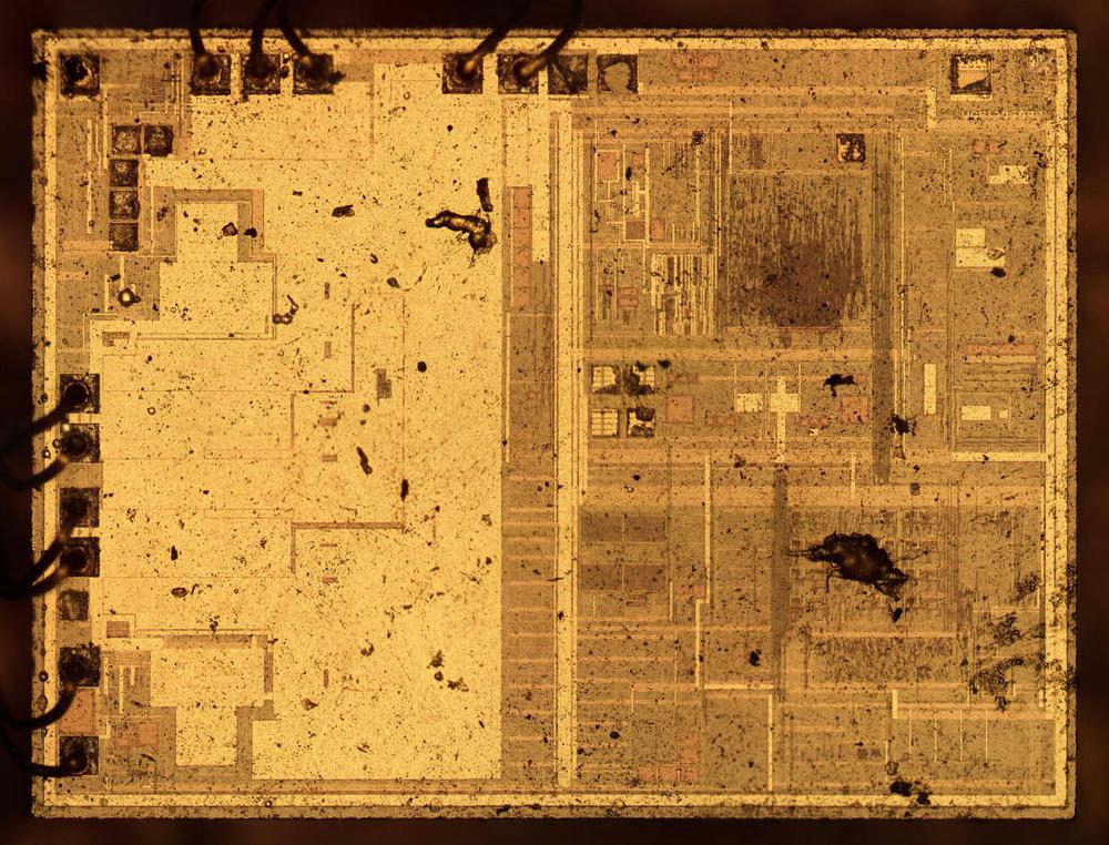
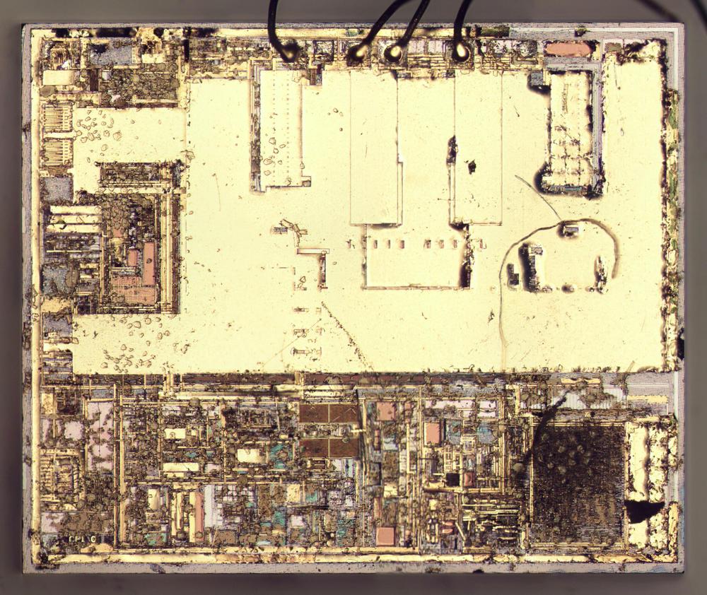
The chip contains two silicon dies, one for the primary-side circuitry that receives power and one for the secondary-side circuitry that outputs power. The photo below shows the silicon die for the secondary. The metal layer on top of the chip is visible; I think there are three metal layers in total to provide the chip's wiring. The chip's silicon is not visible in this photo as it is hidden under the metal. At the top and left, bond wires are connected to pads on the die. The left half of the chip is covered with a lot more metal than the right; the left side has the analog power electronics, so it needs high-current wiring.
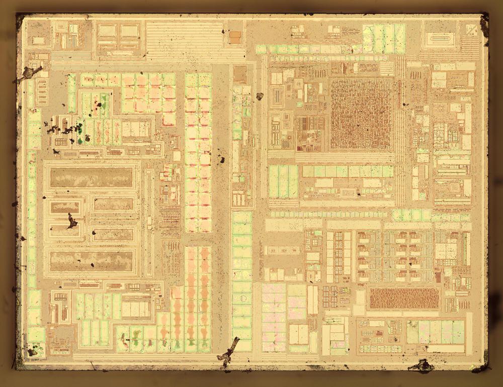
Removing the metal layers5 reveals the underlying silicon (below). This shows the transistors, resistors, and capacitors that make up the chip. There's not a lot of visual similarity between the metal layer and the underlying silicon, but a few of the features match up.
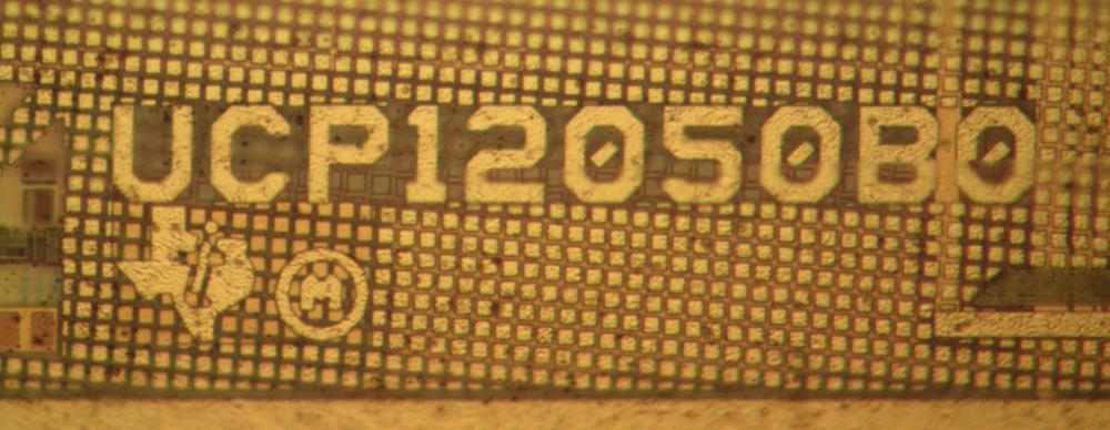
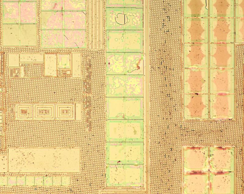
One interesting feature of the chip is "CMP fill". During manufacturing, the layers of the chip were polished flat with Chemical-Mechanical Polishing (CMP). However, regions without any metal wiring are softer and would be polished down too much. To prevent this, empty regions are filled in with a grid of squares, ensuring that the chip is polished to a uniform level. The fill is visible in the photo below as the tiny square boxes at a slight angle. The chip has multiple layers of metal, and each layer has its own fill at a different angle. (The angle prevents the fill from aligning with other features, minimizing stray capacitance and inductance.)
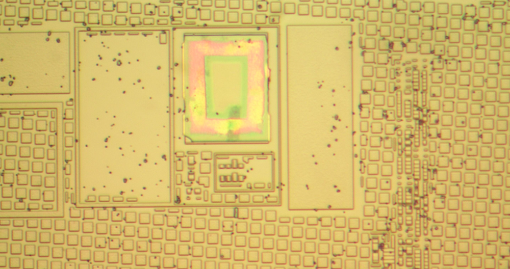
At the bottom of the chip, underneath the metal layers, the silicon also has CMP fill, shown below. These raised fill squares are part of the silicon and the lines between the squares are filled with material, probably polysilicon. Note that although the grid is at an angle, each square is parallel with the chip. In other words, the positions of the squares are at an angle, but not the squares themselves.
The diagram below labels some components of the die. The left side has the power components connected to the transformer, while the right side has the control logic.
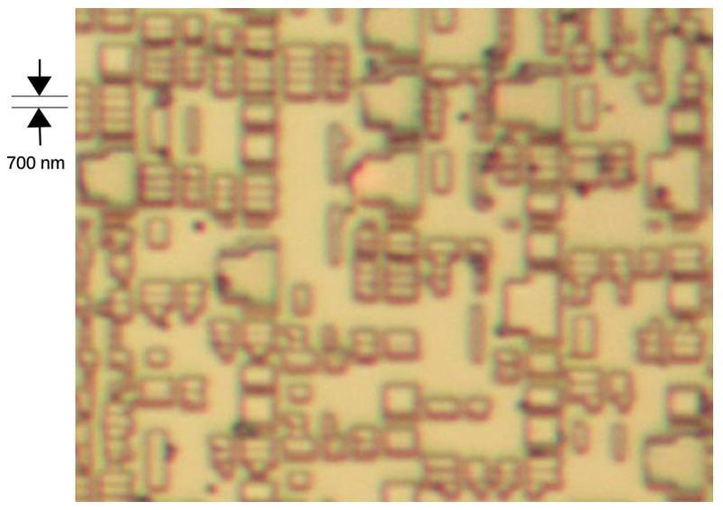
The chip's logic appears to be built from two blocks of standard-cell circuitry, where each logic element is a fixed design from a library, and these cells are arranged on a grid. The photo below shows a closeup of the silicon implementing this logic. Each block is an MOS transistor, wired together by the metal layers that were on top. The smallest visible features are about 700 nm wide, the wavelength of red light. (This explains why the image is fuzzy.) In comparison, cutting-edge chips are now moving to a 5 nm process, 140 times smaller.
A large area of the chip consists of capacitors, which are constructed from a metal layer over the silicon, separated by dielectric. The large square regions in the photo below are capacitors; the dielectric appears yellowish, reddish, or greenish, depending on its thickness. These capacitors are connected together by the metal layer to form larger capacitors. (The tiny square pattern between the capacitors is CMP fill, discussed earlier.) I couldn't dissolve the dielectric, so I suspect it is silicon nitride, rather than the silicon dioxide that provides most of the insulation between the die's layers.
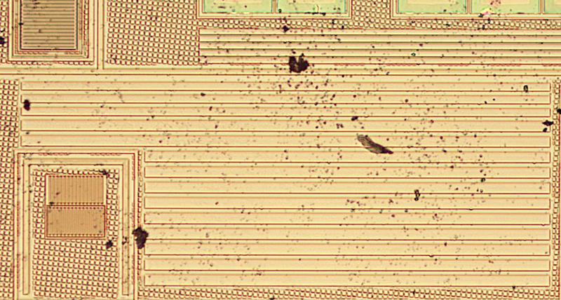
The horizontal stripes in the silicon below are resistors, formed by doping silicon to produce regions with higher resistance. The resistance is proportional to the length divided by the width, so resistors are long and thin to obtain significant resistance. By connecting the resistor stripes at the ends in a zig-zag pattern, a high-value resistor can be produced.
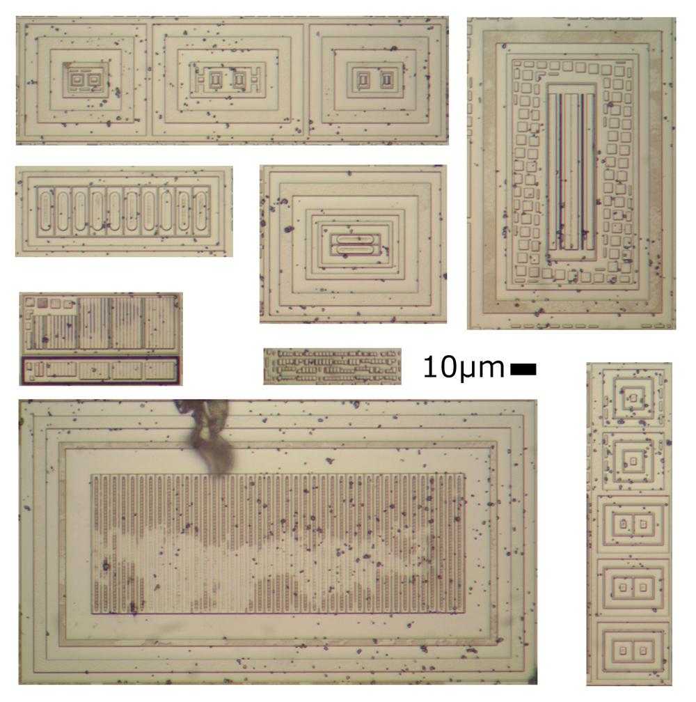
The photo below shows some of the transistors on the chip. The chip uses a wide variety of transistors, ranging from the large power transistor at the bottom to the collection of tiny logic transistors to the left of the "10µm" label. All the transistors are shown at the same scale, so you can see the dramatic range in sizes. (There might be diodes in here too.)
The primary die
The photo below shows the primary-side silicon die. Some of the bond wires are attached to the chip at the top. In this photo, some of the metal layer has been removed, showing the underlying wiring. The top side of the chip has the analog power circuitry, mainly capacitors, and it is covered with a mostly-uniform layer of metal.6
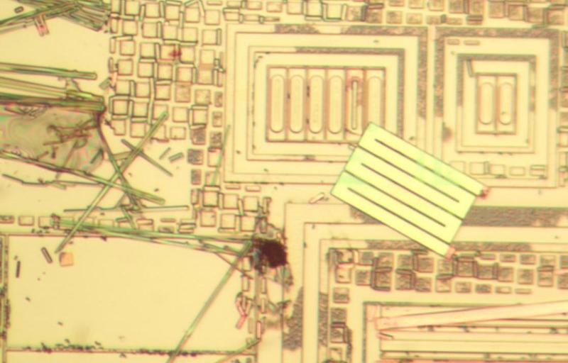
The closeup below shows the primary die midway through removal of the metal and oxide layers. Note that some metal and polysilcon pieces have come loose from the die and are at random angles. This illustrates how the die has a three-dimensional structure, with multiple layers on top of each other. With the oxide removed, the structures in a layer can fall off.
How the chip works
The basic idea of the chip is straightforward; it operates as an isolated DC-DC converter. The primary side of the chip converts the input voltage into pulses that are fed into the transformer. The secondary side rectifies the pulses to produce the output voltage. Because there is no electrical connection between the primary and secondary—just the transformer—the output voltage is electrically isolated. However, the details are not documented: there are many possible "topologies" for generating and rectifying the pulses, such as a flyback converter, a forward converter, or a bridge converter. Another question is how the output voltage is controlled.7
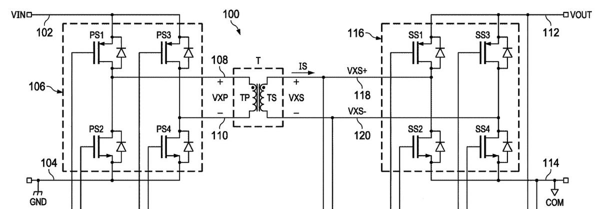
I studied various TI patents, and I think the chip uses a technique called a "phase-shifted dual-active-bridge", shown below. The primary uses four transistors configured as an H-bridge (on the left) to send positive and negative pulses to the transformer (middle). A similar H-bridge on the secondary side (right) converts the transformer's output back to DC. The reason to use an H-bridge instead of diodes on the secondary side is that by changing the timing, more or less power gets transmitted. In other words, by shifting the phase between the primary's bridge and the secondary's bridge, the voltage can be regulated. (Unlike most converters, neither the pulse frequency nor the pulse width is modified in this approach.)
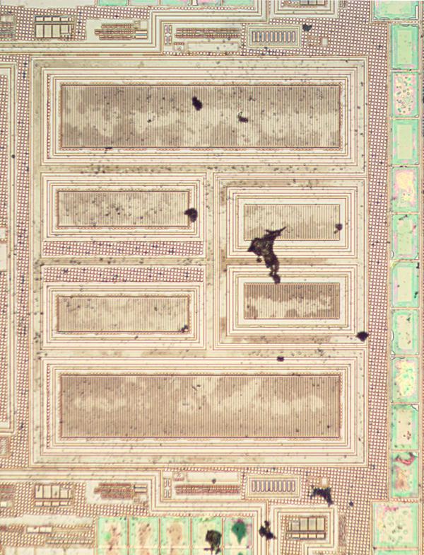
Each H-bridge consists of four transistors: two N-channel MOS transistors and two P-channel MOS transistors. The photo below shows six large power transistors that take up a large fraction of the secondary die. Examining their structure, I think the two on the right are N-channel MOSFETs and the other four are P-channel MOSFETs. This would yield the four transistors required for the H-bridge, with two transistors left over for another purpose.
Using the chip
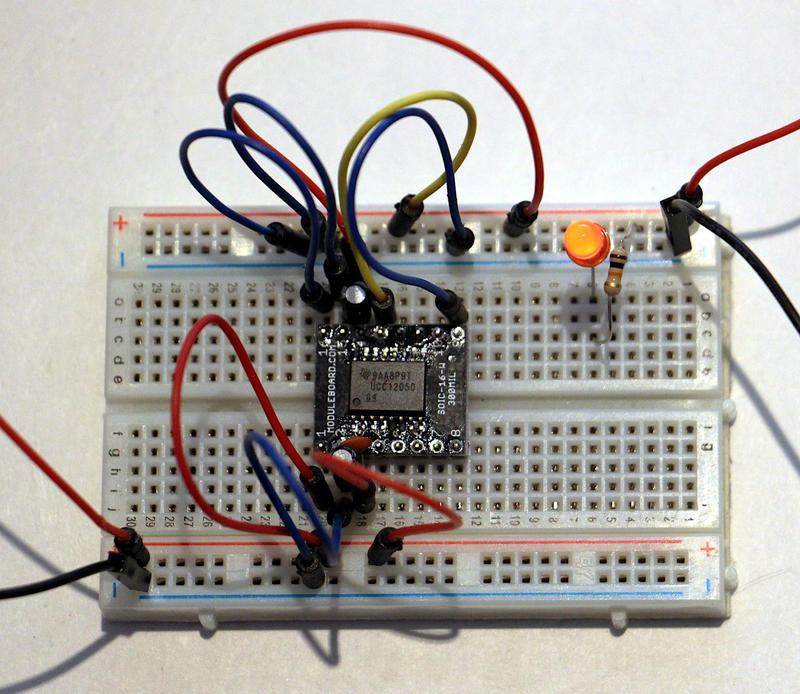
I wired up the chip on a breadboard (below) and it worked as advertised. It's an extremely easy chip to use, just a couple of filter capacitors on the input and output. (While the dies contain numerous capacitors, they are much too small for filtering. External capacitors provide larger capacitances.) I put 5 volts in (lower left) and got 5 volts out (upper right), lighting an LED. When implementing power electronics, it is important to follow layout recommendations to avoid noise and oscillation. However, even though this breadboard did not satisfy any of these recommendations, the chip worked fine. I measured the output at 5 volts, with little noise.
Conclusion
When I saw a chip containing a complete DC-DC converter, I figured there must be some interesting technology inside. Decapping the chip revealed the components, including two silicon dies and tiny planar transformer windings. By studying the pieces and comparing with Texas Instrument patents, I concluded that the chip uses a phase-shifted dual-active-bridge topology for power transfer. (Interestingly, this topology is becoming popular for electric vehicle chargers, although at much higher power.8)
The dies are complex with three layers of metal and small features that can't be resolved optically. I usually examine chips that are decades older and much easier to understand, so this post has more speculation than my typical reverse-engineering. (In other words, I probably got some things wrong.) If you're familiar with modern IC components and recognize any components, please let me know.
I announce my latest blog posts on Twitter, so follow me @kenshirriff for future articles. I also have an RSS feed. Thanks to Robert Baruch for decapping this chip for me and thanks to Texas Instruments for supplying me with a free sample chip.
Notes and references
-
A lot of people complain about ad targeting, but in this case, the ad (below) was an exact match for my interests. This chip is the UCC12050; the datasheet is here.
Texas Instruments' ad for the power transfer chip, showing how small the chip is. -
The chip can output 5V, 3.3V, 5.4V, or 3.7V, selectable by a resistor. The 5.4V and 3.7V values may seem random, but the motivation is they provide an extra 0.4V, allowing the voltage to be regulated by an LDO regulator. The chip doesn't provide a lot of power, just half a watt. ↩
-
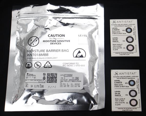
Because of the internal structures in the chip, there is a risk of moisture penetrating the package and accumulating inside. When soldering the chip, this moisture could vaporize, causing the chip to pop like popcorn. To avoid this possibility, the chip was packaged in a special moisture-proof bag that contained moisture indication cards. The chip has moisture sensitivity level 3, indicating it must be soldered within a week of removal from the bag. If the chip exceeds the limit, it must be baked before soldering to drive out the residual moisture.
The moisture-proof bag that held the chip and the moisture indication cards. -
It would be interesting to take a cross-section of this chip to see the exact internal layout, like the cross-sections done by @TubeTimeUS. ↩
-
To remove the layers from the chip, I alternated application of hydrochloric acid (pool acid) to dissolve the metal and application of Armour Etch to remove the silicon dioxide layer. ↩
-
I accidentally dropped the primary die down the drain while trying to clean it, so I don't have many pictures of the primary die. ↩
-
Controlling the output voltage in a DC-DC converter can be done in various ways. A common approach is to send feedback from the secondary side to the primary side through an optoisolator, allowing the primary side to adjust the voltage. In another approach, the primary side uses a separate transformer winding to monitor the voltage. Neither of these approaches seems possible with this chip, though: there's no feedback path from the secondary, but the output voltage is selected by the secondary. An inefficient approach would be to put a linear voltage regulator on the secondary side to drop the voltage to the desired value. ↩
-
I came across an interesting video that shows a dual-active-bridge converter for electric vehicle charging. This converter is powered directly from a 2.5-kilovolt power line, which is a bit scary. ↩


Fascinating read, well done!
ReplyDeleteGreat article!
ReplyDeleteInteresting IC for portable audio devices which get power over USB.
ReplyDeleteVery informative, thanks for the article. Also, it's Good to know TI is keeping innovation alive.
ReplyDeleteBrilliant analysis. Many thanks for an interesting read.
ReplyDeleteSuper study
ReplyDeleteGreat article!
ReplyDeleteany idea about RFI?
Thanks Ken. loved to see the teardown
ReplyDeleteThis is one of the few blogs where paragraph two can begin with a casual discussion of boiling something in sulphuric acid at 210c, and it doesn't feel strange.
ReplyDelete