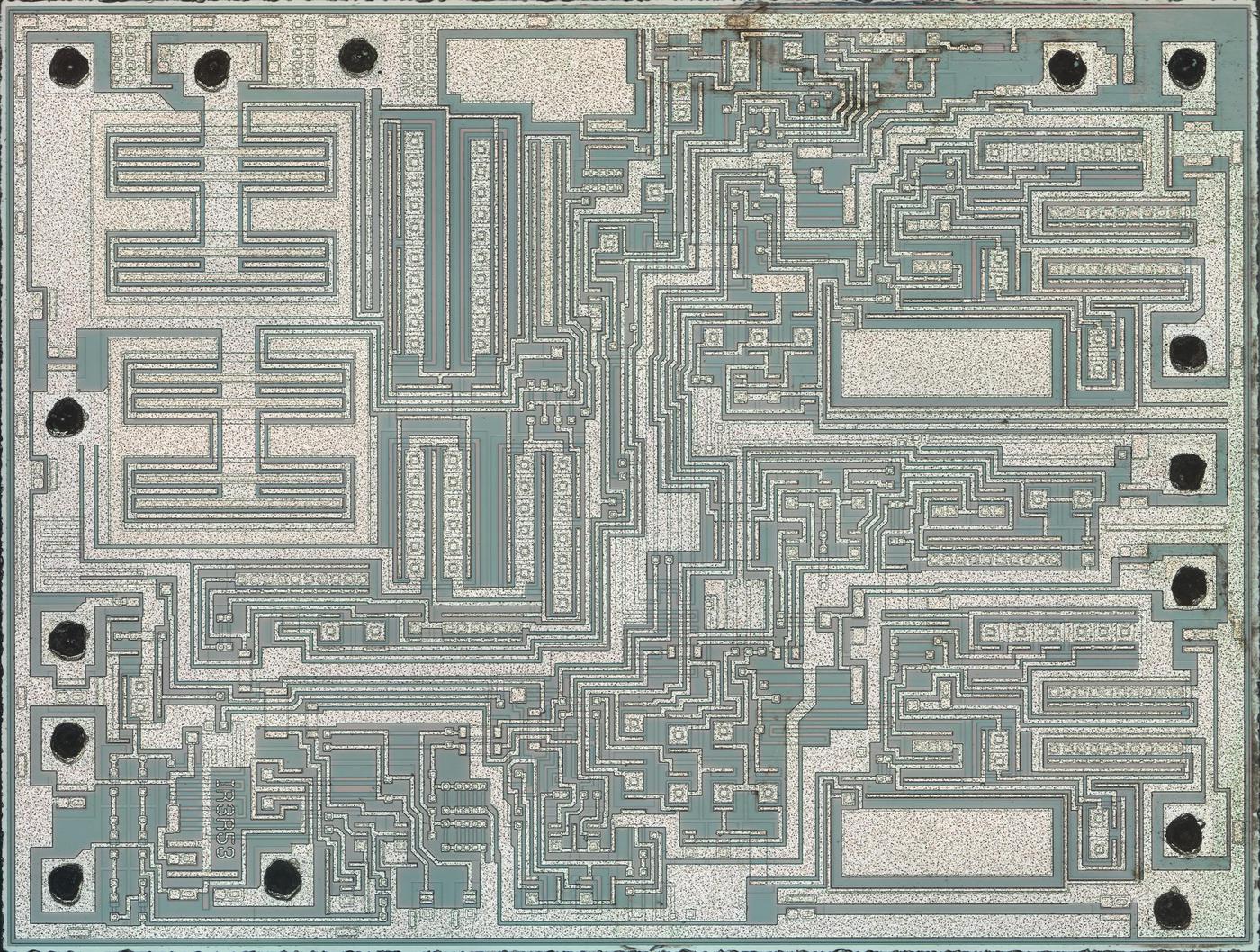
The Nintendo Game Boy Color is a handheld game console that was released in 1998. It uses an audio amplifier chip to drive the internal speaker or stereo headphones. In this blog post, I reverse-engineer this chip from die photos and explain how it works.1 It's essentially three power op-amps with some interesting circuitry inside.
The photo above shows the chip's silicon die as it appears under a microscope. The white lines are the chip's metal layer, connecting the components. The silicon itself appears greenish and is underneath the metal. The black circles around the outside are the bond wire connections, where tiny wires connected the silicon die to the chip's package. Regions of the chip are treated (doped) to change the electrical properties of the silicon. The next sections explain how components are created from these different types of silicon.
NPN transistors
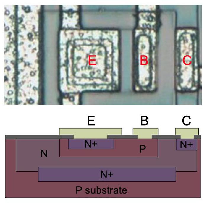
The amplifier chip is built from transistors known as NPN and PNP bipolar transistors, different from the low-power MOS transistors used in processors. These transistors have three connections: the emitter, the base, and the collector. The magnified photo below shows one of the transistors as it appears on the chip. The slightly different tints in the silicon indicate regions that have been doped to form N and P regions, with dark lines separating the regions. The bubbly silverish areas are the metal layer of the chip on top of the silicon—these form the wires connecting to the collector, emitter, and base.
Underneath the photo is a cross-section drawing illustrating how the transistor is constructed. The emitter (E) wire is connected to N+ silicon. Below that is a P layer connected to the base contact (B). And below that is an N+ layer connected (indirectly) to the collector (C). If you look at the vertical cross-section below the 'E', you can find the N-P-N layers that form the transistor.
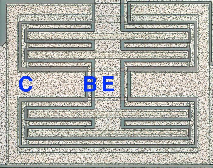
The photo below shows one of the large output transistors used to drive the speaker. These transistors must produce a high-current output, so they are much larger than the regular transistors and have a different structure. Note the multiple interlocking "fingers" of the emitter and base, surrounded by the large collector. If you look back at the die photo, you can see two of these transistors filling the upper left part of the die.
PNP transistors
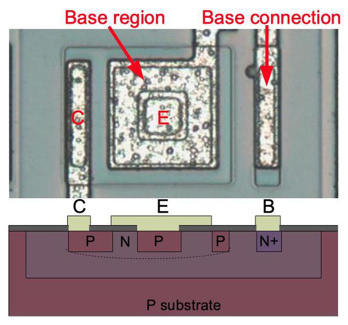
The chip also uses PNP transistors, which have an entirely different construction, as shown in the diagram below.2 The PNP transistor has a small square emitter (P-silicon), surrounded by a square base region (N-silicon), which in turn is surrounded by the collector (P-silicon). (The emitter metal covers both the emitter and the base, but is only connected to the emitter.) These regions form a P-N-P sandwich horizontally (laterally), unlike the vertical structure of the NPN transistors. Note that although the base region physically surrounds the emitter, the metal connection to the base is further away; the base signal passes through the N and N+ regions, underneath the collector, to reach the base region.
How resistors are implemented in silicon
Resistors are an important component of analog chips. The photo below shows a long, zig-zagging resistor, connected to metal wiring at the bottom of the photo. (The resistor passes under the metal layer at several points.) The resistor is formed as a strip of P silicon. The resistance is proportional to the length of the resistor, so large-value resistors have a zig-zag shape to fit in the available space. Because resistors are relatively large and inaccurate, chip designs try to minimize the number of resistors required. Even so, an analog chip like this one requires numerous resistors.
Capacitors
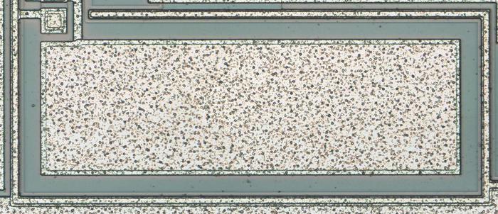
This chip has three large capacitors, one for each amplifier. The photo below shows one of the capacitors. The capacitors are simply a layer of metal over the underlying silicon, separated by a thin insulating oxide layer. In this chip, capacitors are used to ensure the stability of the amplifiers. Because they are large, the three capacitors are easy to spot in the chip die photo.
The chip and the Game Boy Color
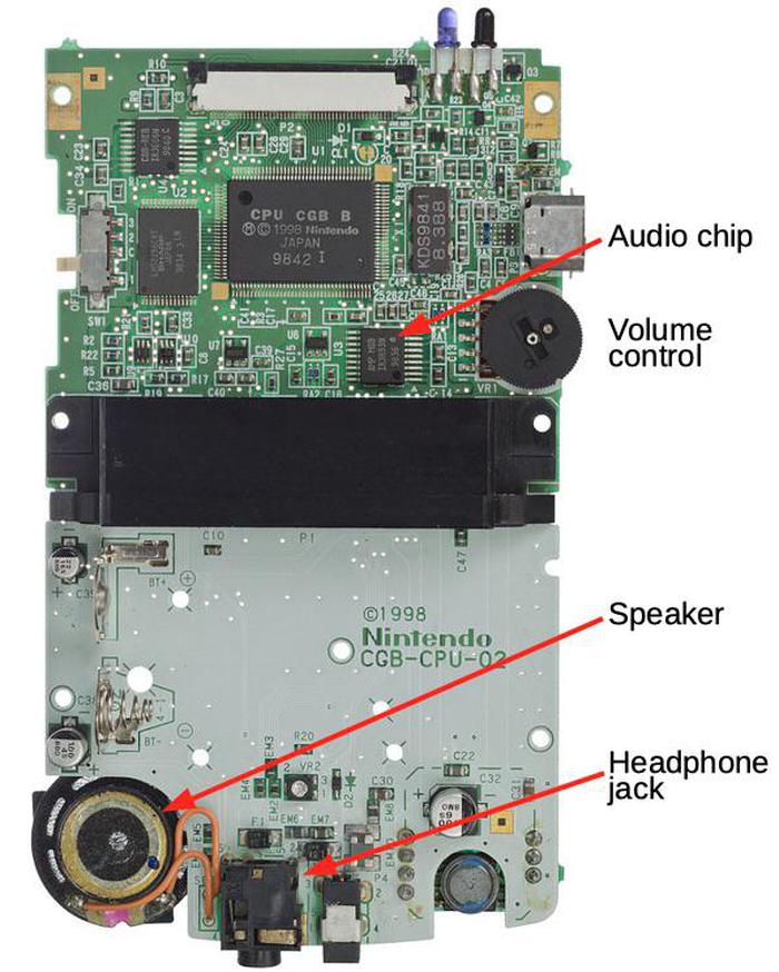
The role of the audio chip is to take the sound generated by the CPU and amplify it, either for the internal speaker or for external headphones. The photo below shows how the chip appears on the Game Boy motherboard. It also shows the speaker, headphone jack, and the volume control that adjusts the input levels to the amplifier chip.
The chip contains three audio amplifiers: one for the speaker and two for the headphones (because they have left and right channels). The design of these three amplifiers is almost identical, except the speaker amplifier uses larger transistors for more output power. The amplifiers use an op-amp, a type of amplifier that uses negative feedback to control the level of amplification. (The feedback resistors are internal to the chip, but it uses external capacitors for filtering.4)53
IC circuits: The current mirror
There are some subcircuits that are very common in analog ICs, but may seem mysterious at first. The current mirror is one of these. The idea is you start with one known current and then you can "clone" multiple copies of the current with a simple transistor circuit, the current mirror. A common use of a current mirror is to replace resistors. As explained earlier, resistors inside ICs are both inconveniently large and inaccurate. It saves space to use a current mirror instead of a resistor whenever possible. Also, the currents produced by a current mirror are nearly identical, unlike the currents produced by two resistors.
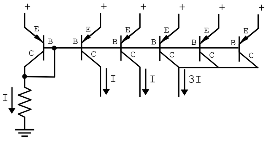
The following circuit shows how a current mirror implemented with PNP transistors.6 A reference current "I" passes through the transistor on the left. (In this case, the current is set by the resistor.) Since all the transistors have the same emitter voltage and base voltage, they source the same current, so the currents through each transistor match the reference current on the left. In this mirror, the three transistors on the right are connected so the total output is 3I. Thus, by using multiple transistors, currents can be generated with precise ratios.
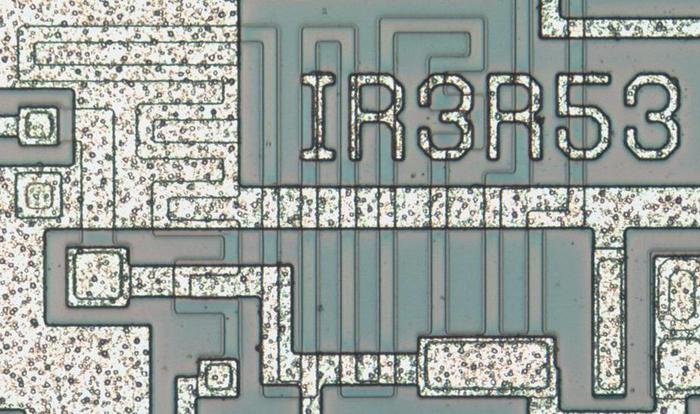
The photo above shows how that current mirror is implemented on the chip with six PNP transistors. Their bases are all connected (top thin metal strip) as are their emitters (wide central middle strip). The leftmost transistor has its base and collector connected, so it controls the current mirror.
IC component: The differential pair
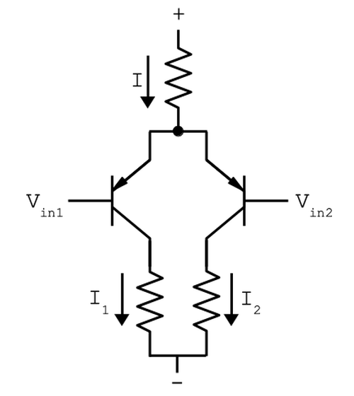
The second important circuit to understand is the differential pair, the most common two-transistor subcircuit used in analog ICs. 7 The differential pair is the basis of an op-amp: it takes two voltages, computes their difference, and amplifies the result. The schematic below shows a simple differential pair. The resistor at the top provides a fixed current I, which is split between the two input transistors. If the input voltages are equal, the current will be split equally into the two branches (I1 and I2). If one of the input voltages is a bit higher than the other, the corresponding transistor will conduct more current, so one branch gets more current and the other branch gets less. The load resistors at the bottom produce an output voltage depending on the current.
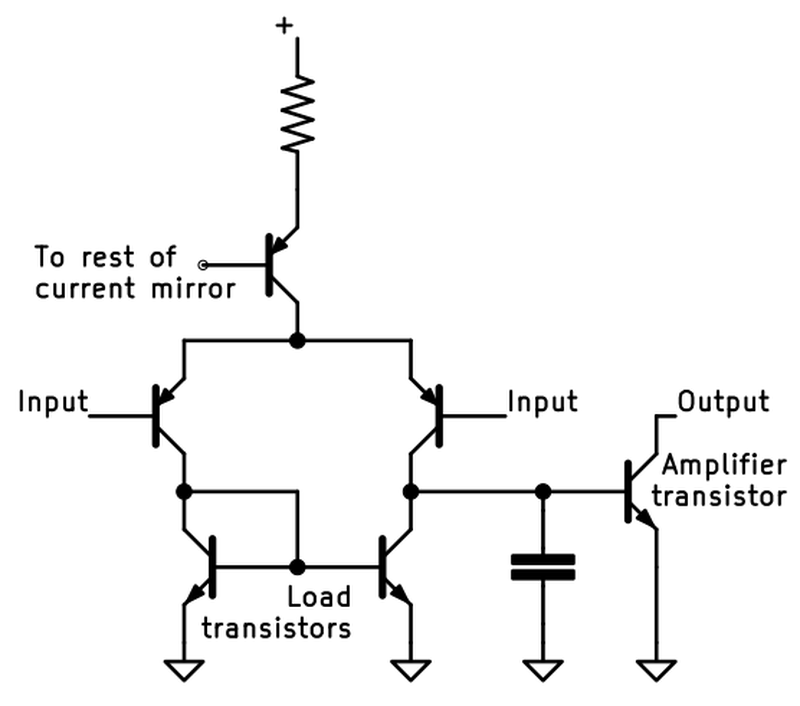
To improve performance, a differential pair is implemented as shown below. A current mirror at the top provides the fixed current. The two load resistors at the bottom of the differential pair have been replaced by load transistors. The output is taken from one branch of the differential pair and fed into a transistor for more amplification. The output then goes to the amplifier's high-current output stage (not shown). A compensation capacitor stabilizes the circuit.
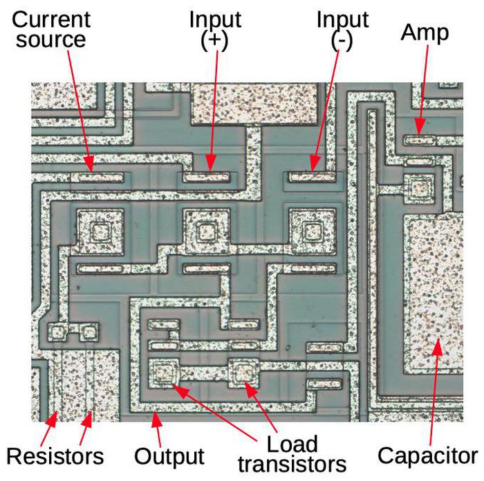
The diagram below shows the implementation of a differential pair in silicon, corresponding to the schematic above. The circuit has three larger PNP transistors above and three smaller NPN transistors. By following the metal, it can be seen how the circuit corresponds to the schematic.
Layout of the chip
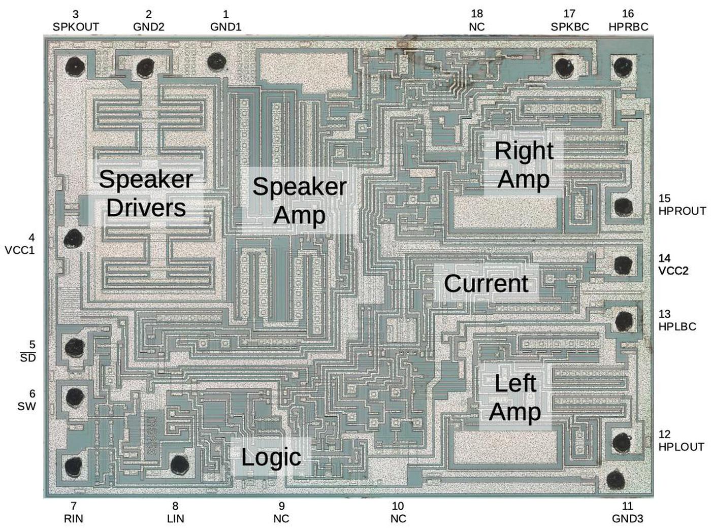
The diagram below shows the main functional blocks of the chip. The upper-left part of the chip has the two large driver transistors for the speaker output (one to pull the signal low and the other to pull the signal high). The remaining circuitry for the speaker amplifier includes the differential pair, current mirrors, and other circuits. The headphone amplifier consists of two nearly-identical blocks: one for the left channel and one for the right. The circuitry for the current sources and current mirrors is shared by both headphone channels. The lower-left of the chip contains digital logic to enable the speaker amp or the headphone amp, depending if a headphone is plugged into the jack and depending on the enable pin.
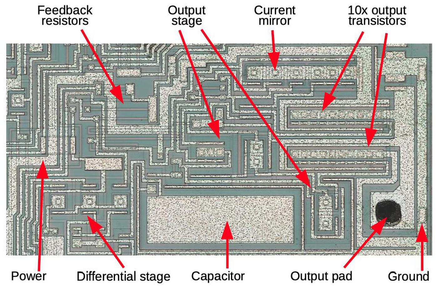
Zooming in on the upper-right corner shows the amplifier circuitry for one of the headphone channels. The input signal goes through the differential stage (discussed earlier) and amplification, before going to the output stage, which consists of multiple transistors. Although the speaker amp uses large output transistors, the headphone amp uses 10 regular transistors in parallel; one set to pull the output high and the second to pull the output low. Resistors are used to generate the negative feedback signals for the amplifier. Note that power and ground use much thicker metal traces to support the necessary current.
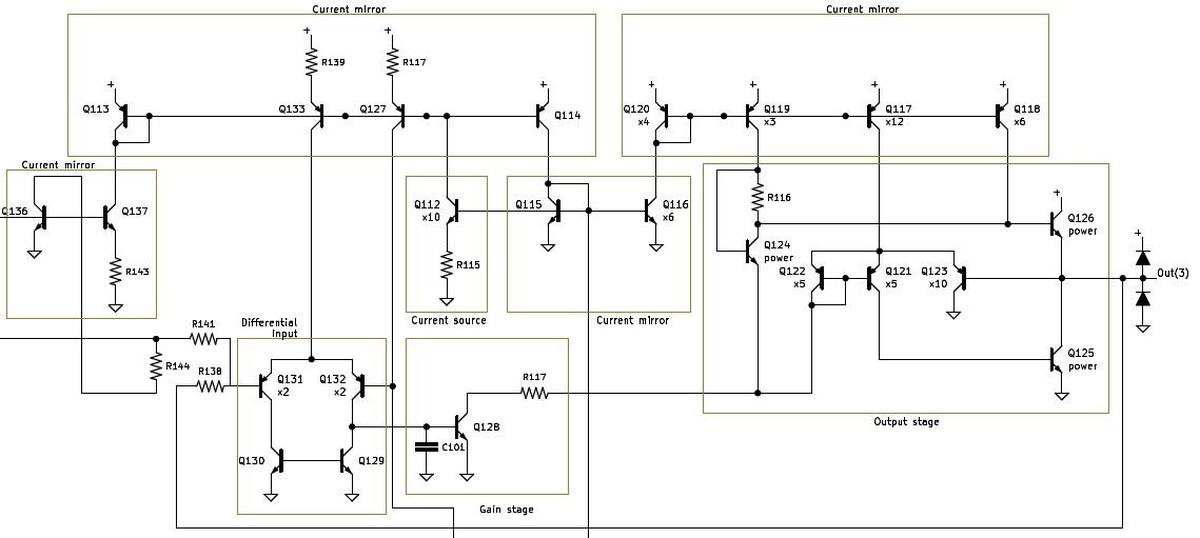
I created a complete schematic of the chip here. I won't explain it in detail here, since its op-amps use a standard architecture, but I'll point out some highlights.9 The headphone amplifiers and the speaker amplifier have very similar designs, but there are a few differences. Most notably, the speaker transistors are larger because the speaker requires more current: not just the output transistors, but many of the other transistors in the circuit. The current mirrors are also structured slightly differently between the headphone amplifiers and the speaker.8 Unlike many amplifier chips, this chip doesn't appear to have any protection if the output is short-circuited.
Conclusion
This amplifier chip from 1998 has about 100 transistors and is simple enough that the circuitry can be traced out under a microscope. (In comparison, a Pentium II processor from the same time had 7.5 million transistors.) The chip illustrates important analog design functions such as the differential pair and current mirror, and how they can be combined to build an amplifier. People have reverse-engineered many Nintendo chips to help build Nintendo emulators. I don't think knowing the audio chip circuitry helps with emulation, but it's interesting to see how it is constructed.
I announce my latest blog posts on Twitter, so follow me @kenshirriff for future articles. I also have an RSS feed. My KiCad files for the schematic are on Github. Thanks to John McMaster for providing the chip photos; his page is here.
Notes and references
-
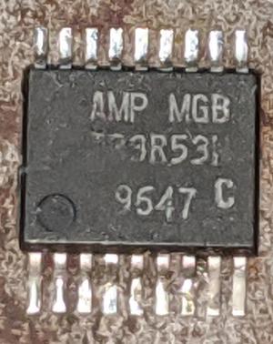
The audio chip is labeled AMP MGB, presumably for "amplifier, Mini-Game Boy". The part number on the 18-pin chip is IR3R53N.
The IR3R53N chip. Photo courtesy of John McMaster. -
On this chip, the NPN transistors and PNP transistors look superficially similar, but the PNP transistors are considerably larger. The PNP transistors can also be distinguished by the wide base ring under the square emitter metal. ↩
-
One interesting thing about the chip is that it has three ground pins (1, 2, and 11), and two power pins (4 and 14). By examining the chip, we can why there are multiple pins. Most of the chip uses the pin 1 ground. The pin 2 ground is used solely for the speaker output transistor. The pin 14 ground is used by the headphone driver circuitry. The separate grounds prevent transients from the high-current output transistors from affecting the rest of the chip. For the power pins, most of the chip uses pin 4, while pin 14 feeds the various current sources. This ensures the current sources remain stable. ↩
-
I believe the three external filter capacitors implement a high-pass filter for each channel. ↩↩
-
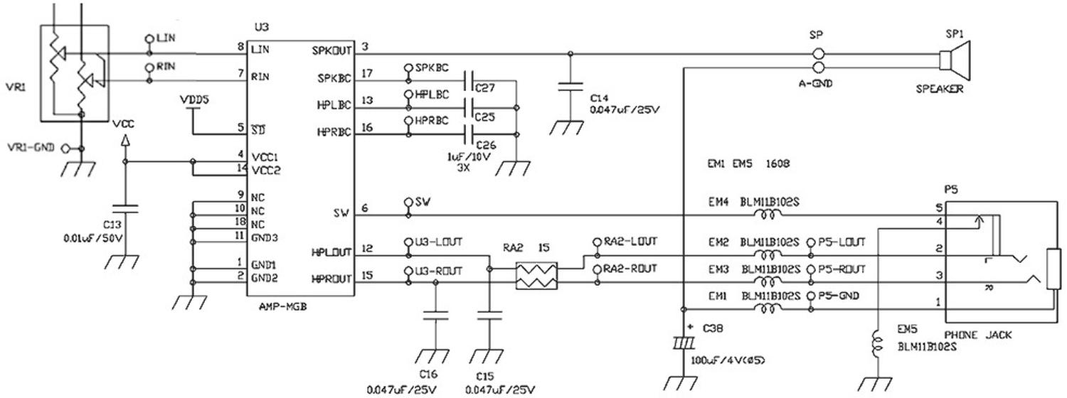
The excerpt from the Game Boy Color Schematic below shows how the audio chip is connected. The Game Boy CPU chip provides left and right audio channels to the audio chip inputs (LIN and RIN). The chip provides a single-channel speaker output SPKOUT. It also provides two-channel headphone output: HPLOUT and HPROUT. Each channel has an external capacitor attached for filtering: SPKBC, HPLBC, and HPRBC.4 When headphones are plugged in, this signals the SW pin, causing the chip to switch from the speaker output to the headphone outputs. The SD pin allows the chip to be disabled, but is unused.
Schematic showing the audio chip's role in the Game Boy Color. From Consoles TechWiki.On the left, the chip receives the audio inputs from the CPU, via a volume control. On the right, the chip is connected to the speaker and headphone jack. The filter capacitors are also connected on the right. The SW input is connected to a switch in the headphone jack; it is normally grounded, but disconnected when headphones are inserted into the jack. ↩
-
For more information about current mirrors, check Wikipedia or chapter 3 of Designing Analog Chips. ↩
-
According to Analysis and Design of Analog Integrated Circuits differential pairs are "perhaps the most widely used two-transistor subcircuits in monolithic analog circuits" (p214). For more information about differential pairs, see Wikipedia or chapter 4 of Designing Analog Chips. ↩
-
The headphone amp or speaker amp are disabled by shutting down their respective current mirrors. Some of the current mirrors remain partially powered, rather than shutting down completely. ↩
-
The amplifiers use a fairly complex scheme to bias and drive the two output transistors. I'll explain my understanding of it; follow along with the schematic. A standard approach is to use diodes to achieve the biasing. However, this chip uses a complex current mirror setup. Looking at the speaker amplifier circuit, transistor Q128 provides the main amplification. The current sunk by this transistor controls the output. The output pull-up transistor Q126 receives base current from current sources Q118 and Q119. This base current can instead flow through Q124 and Q128 if Q128 is conducting, shutting off Q126. At the same time, if Q128 is conducting, the current through it will be (partially) mirrored by Q122, causing current flow through Q121 to turn on pull-down output transistor Q125. To turn off Q125, this current will flow through Q123 instead. To summarize, if Q128 is conducting, Q125 turns on and the output is pulled low. If Q128 is not conducting, Q126 turns on and the output is pulled high. In between, the output will be linear. (I couldn't find references to this approach anywhere, so please let me know if you have more details about this amplifier configuration.) ↩

4 comments:
Congratulations on the article!
It is very good to read something good and profound. I'm an electronics technician (and electrical engeneering student) and I didn't even thought it was possible to reverse-engineering of an IC.
But a sad point: I am from Brazil, and here we have only one chip factory, which produces only two chip models. If I wanted to replicate this 1998 model, I would have to have it manufactured outside the country, because here we have no way, for now.
Best regards!
In the circuit diagram, it seems a bridge betweeb B and E of either Q130 or Q129 is missing.
Congratulations. A good work.
Hello, nice work!!
In the PNP transistors section, there is this: (The emitter metal covers both the emitter and the base, but is only connected to the "base"), I think you meant : ....only connected to the "emitter", no?!
Post a Comment