Inside the Am2901: AMD's 1970s bit-slice processor

You're probably familiar with modern processors made by Advanced Micro Devices. But AMD's processors go back to 1975, when AMD introduced the Am2901. This chip was a type of processor called a bit-slice processor: each chip processed just 4 bits, but multiple chips were combined to produce a larger word size. This approach was used in the 1970s and 1980s to create a 16-bit, 36-bit, or 64-bit processor (for example), when the whole processor couldn't fit on a single fast chip.1

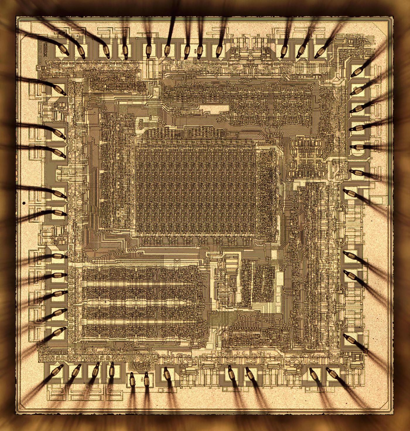
Die photo of the Am2901 chip.
This image shows the metal layers of the chip; the silicon is underneath. Around the edges of the die, tiny bond wires connect the chip to the external pins.
(Click the photo for a high-res image.)

Die photo of the Am2901 chip. This image shows the metal layers of the chip; the silicon is underneath. Around the edges of the die, tiny bond wires connect the chip to the external pins. (Click the photo for a high-res image.)

The Am2901 chip became very popular, used in diverse systems ranging from the Battlezone video game2 to the VAX-11/730 minicomputer, from the Xerox Star workstation to the F-16 fighter's Magic 372 computer.3 The fastest version of this processor, the Am2901C, used a logic family called emitter-coupled logic (ECL) for high performance. In this blog post, I open up an Am2901C chip, examine its die under a microscope, and explain the ECL circuits that made its arithmetic-logic unit work.

The bit-slice processor

You might wonder how multiple processor chips could work together to support arbitrary word lengths. The key is that a bit-slice processor is a building block, rather than a complete processor,6 and requires separate circuitry to decode instructions and control the system.4 The bit-slice processor chips performed arithmetic or logic operations on the data and contained registers, while a control chip (such as the Am2910) told the bit-slice chips what to do. Each machine instruction was broken down into smaller steps called micro-instructions which were stored in a microcode ROM. Note that the computer's instruction set was defined by the microcode, not by the Am2901, so almost any instruction set could be supported.5

Bit-slice processors fell in between using a microprocessor chip and building a computer out of simple TTL chips. Building a processor out of TTL chips was much faster than a microprocessor at the time, but required boards full of chips. Using a bit-slice processor kept the speed advantage, but reduced the chip count. The bit-slice processor also provided much more flexibility than a microprocessor, allowing the designer to customize the instruction set and other architectural features.

An overview of the die

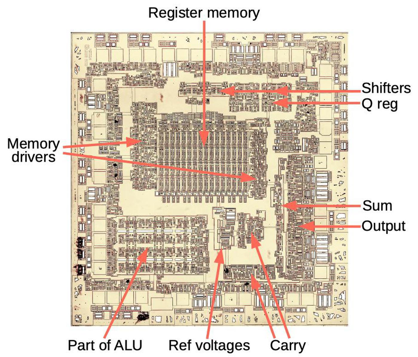
The photo below shows the Am2901 die, with key functional blocks labeled.7 For this photo, I removed the metal layers so you can see the silicon and the transistors.8 The largest functional block of the chip is the register memory in the center. The chip has sixteen 4-bit registers. (If you look closely, you can see 16 columns and 4 rows in the memory array.) To the left and right of the memory block are the memory driver circuits that read and write the memory.

Die photo of the Am2901 chip with main functional blocks labeled. The circuitry around the outside largely consists of buffers to convert between the external TTL signals and the internal ECL signals.

Die photo of the Am2901 chip with main functional blocks labeled. The circuitry around the outside largely consists of buffers to convert between the external TTL signals and the internal ECL signals.

The chip's arithmetic-logic unit (ALU) performs arithmetic operations (addition or subtraction) or logical operations (And, Or, Exclusive-or). The first section of the ALU is a large block in the lower left of the chip; it consists of four rows since it is a 4-bit ALU. The ALU also contains logic to generate the carry outputs for addition, using a fast technique called carry lookahead.9 Next, the ALU uses the carry values to generate the sum in parallel. Finally, the output circuitry processes and buffers the sum and sends it to the output pin.

The empty squares near the edge of the chip are the pads that connect the chip to the outside world. Next to the pads is the circuitry to send and receive signals. In particular, since the chip communicates with external circuits using TTL signals, but uses ECL circuitry inside, this circuitry converts between TTL and ECL voltages.

The chip has two shifters that can shift a word one bit to the left or right. The Q register is a 4-bit register built from flip flops. Finally, the reference voltage circuitry generates the precision voltage references required by the ECL logic.

How to see the die

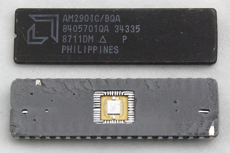
To see what's inside a chip usually requires dissolving the plastic case with dangerous acids. However, I bought an Am2901 chip that came in a ceramic package instead of plastic. By simply tapping the chip's seam with a chisel, I popped the two halves of the chip apart, exposing the die inside. The silicon die is the small square in the center of the chip. Thin bond wires connect the pads on the die to the lead frame, which goes to the 40 external pins of the chip.

The Am2901 after separating the two halves of the ceramic package.

The Am2901 after separating the two halves of the ceramic package.

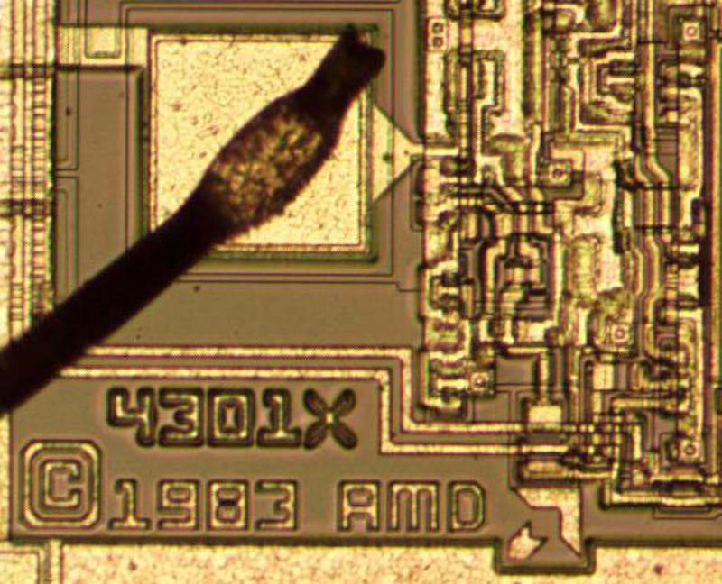
I used a special type of microscope called a metallurgical microscope to take high-resolution photographs of the chip. The photograph below shows the AMD logo. Above is a bond wire connected to a pad. The chip has two layers of metal wiring up the circuitry, visible to the right.

A closeup of the die showing "4301X" (presumably an internal part number) and "© 1983 AMD".

A closeup of the die showing "4301X" (presumably an internal part number) and "© 1983 AMD".

I stitched together multiple microscope photos to create the high-resolution images. I describe my process for creating die photos in more detail here. I then removed the metal layers8 and created another set of images of the silicon.

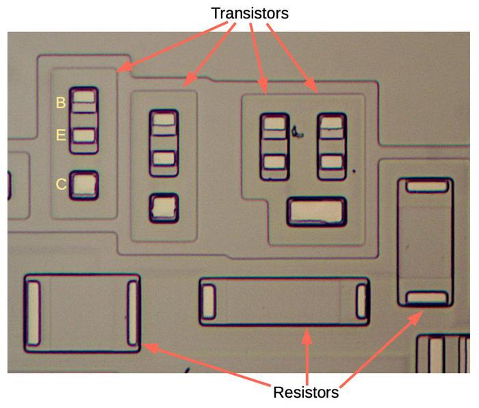
The photo below is a closeup of the silicon, showing four transistors and three resistors. Parts of the silicon are "doped" to give them different properties, and the different doping regions are visible under the microscope. This chip is built with bipolar NPN transistors, different from the MOS transistors in modern computers. The transistor on the left has the base (P-type silicon), emitter (N-type silicon), and collector (N-type silicon) labeled. The whiteish rectangles are the contacts between the silicon and the metal layer which was on top before being removed. The two transistors on the right share a single large collector. On this chip, it is common for multiple transistors to share the collector.

A closeup of the die with metal removed, showing transistors and resistors.

A closeup of the die with metal removed, showing transistors and resistors.

At the bottom are three resistors. A resistor is produced by doping the silicon to increase its resistance. Resistors on integrated circuits generally have poor accuracy. They are also relatively large; these ones are the same size as transistors, while other resistors are even larger. For these reasons, integrated circuit designs try to minimize the number of resistors.

Emitter-coupled logic

Logic circuits can be built in a wide variety of ways. Almost all computers today use a logic family called CMOS (complementary metal-oxide-semiconductor), building gates out of MOS transistors. In the minicomputer era, TTL (transistor-transistor logic) was very popular. Emitter-coupled logic (ECL) was a faster,10 but less common logic family. A disadvantage of ECL was its higher power consumption. (Circuitry in the Cray-2 supercomputer (1985) had to be immersed in Fluorinert coolant because the ECL gates gave off so much heat.)

The first versions of the Am2901 used TTL logic, but in 1979 AMD introduced a faster version, the Am2901C. The Am2901C used ECL logic internally for speed, but supported TTL voltages externally, allowing it to be easily used in TTL computers. The Am2901C, the ECL version, is the one in this blog post.

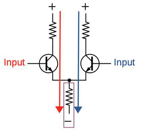
ECL is based on a differential pair, similar to the circuit inside an op-amp. The idea behind a differential pair (below) is that a fixed current flows through the circuit. If the left input is a higher voltage than the right, the left transistor will turn on and most current will flow through the left branch. Conversely, if the right input is a higher voltage than the left, the right transistor will turn on and most current will flow through the right branch. (Note that the emitters of the transistors are coupled together, thus the name emitter-coupled logic.)

A differential pair. If the left input (red) is higher, most of the current flows along the left path.
Conversely, if the right input (blue) is higher, most of the current flows along the right path.

A differential pair. If the left input (red) is higher, most of the current flows along the left path. Conversely, if the right input (blue) is higher, most of the current flows along the right path.

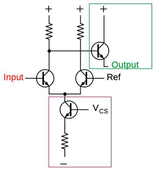
A few modifications turn the differential pair into an ECL gate. First, the voltage into one branch is fixed at a reference voltage, midway between the "0" level and the "1" level. Thus, if the input is higher than the reference voltage, it will be considered a "1", and lower will be a "0". Next, an output transistor (green) is attached to a branch to produce an output by buffering the branch's voltage. The circuit below is an inverter, since if the input is high, the current through the left resistor will pull the output low. To improve performance, the bottom resistor has been replaced with a current sink (purple), built from a transistor and a resistor.11

An ECL inverter. This is based on the differential pair with an output transistor added (green) and the bias resistor replaced with a constant-current circuit (purple). The upper-right resistor can be omitted since no output is connected to it.

An ECL inverter. This is based on the differential pair with an output transistor added (green) and the bias resistor replaced with a constant-current circuit (purple). The upper-right resistor can be omitted since no output is connected to it.

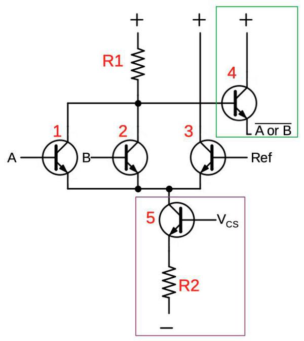
A more complex ECL gate can be created by adding more inputs. In the circuit below, a second input transistor (2) has been added in parallel with transistor 1. The current will go through the resistor R1 if input A or input B are 1 (i.e. higher than the reference voltage). In this case, the output is pulled low, creating a NOR gate. Other circuit configurations can implement AND gates, XOR gates, or more complex logic circuits.12

An ECL NOR gate as implemented on the chip.

An ECL NOR gate as implemented on the chip.

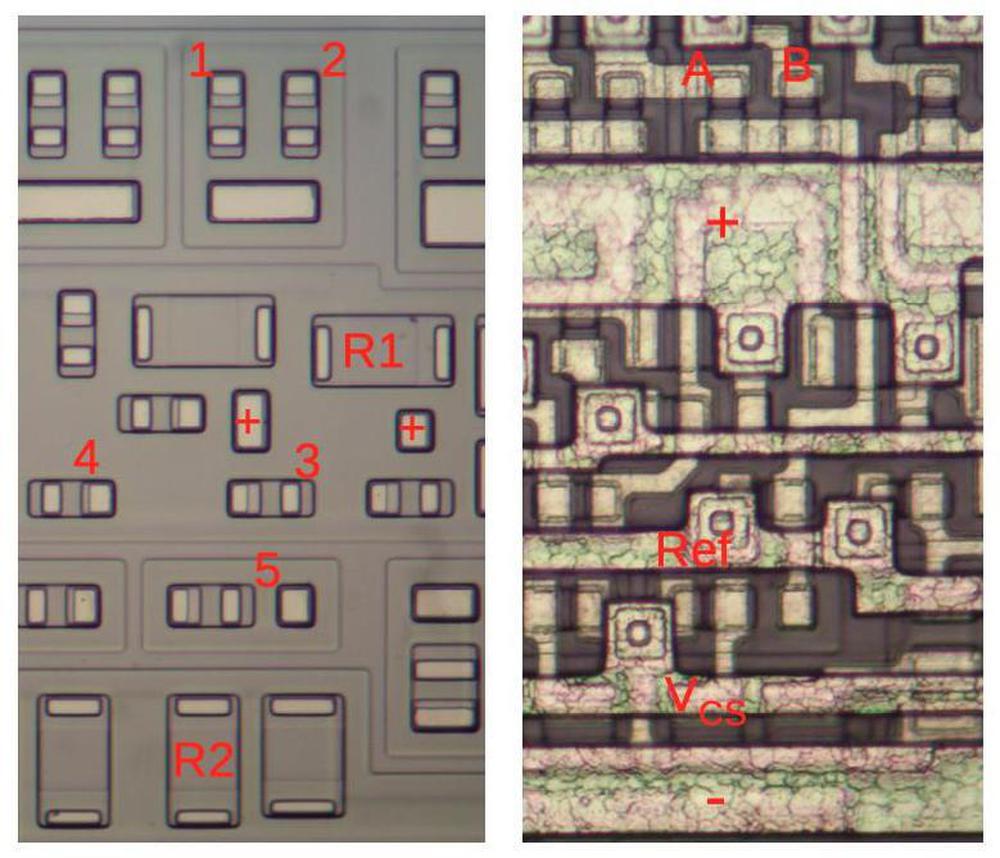
The schematic above shows a NOR gate as implemented on the chip. The photos below show the corresponding physical layout of the gate. On the left is the silicon layer of the die, showing the transistors and resistors. The photo on the right shows the metal wiring for the same part of the chip. At the top of the photo, transistors 1 and 2 receive the inputs to the gate. Each transistor has its base at the top and emitter in the middle. The transistors share a collector, the white rectangle below. The resistors R1 and R2 are the indicated rectangles of silicon. The transistors in the middle (including 3 and 4) all share a collector, connected twice to the positive voltage. (The non-numbered transistors and resistors are parts of other gates.)

A NOR gate as implemented on the Am2901 die.

A NOR gate as implemented on the Am2901 die.

Looking at the wiring on the right, the top layer provides horizontal wiring for the positive supply voltage, reference voltages, the current sink voltage VCS, and the negative (ground) supply voltage. (Note that the suppy and ground are much wider to support higher current.) Underneath this is the wiring connecting the transistors together. At the top, the inputs A and B are wired to the transistor bases. It's harder to trace out the other wiring as it is obscured by the top layer. But, for instance, you can see the connection between transistor 4, the collector of transistors 1 and 2, and R1. By studying the die photos carefully, one can determine all the wiring and reverse-engineer the chip's logic.

The Arithmetic-Logic Unit (ALU)

The arithmetic-logic unit (ALU) in the Am2901 chip performs 4-bit arithmetic or logical operations. It supports 8 different operations: addition, subtraction, and bitwise logic operations.17 (Note that it does not perform multiplication or division.)

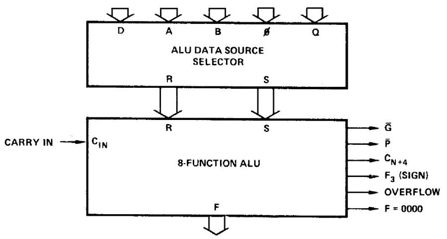
The block diagram below shows the structure of the Am2901's ALU. First, a selector (multiplexer) selects the two inputs to the ALU from the potential sources. "D" is the value fed into the chip's data pins, typically the processor's data bus. (This data first goes through circuitry to convert the external TTL voltage levels used to the ECL voltage levels inside the chip.) "A" is the value of one of the 16 entries in the chip's register file, selected by pins A0-A3, and "B" is similar. The constant value 0 can be fed into the ALU. Finally, "Q" is the contents of the Q register (an extra register, separate from the register file). The multiple data sources give the chip a lot of flexibility.

Block diagram of the Am2901 ALU, from the datasheet. The ALU performs one of eight functions on its two 4-bit inputs: R and S. At the right are various outputs from the chip: G, P, carry out, sign, overflow, and zero test.

Block diagram of the Am2901 ALU, from the datasheet. The ALU performs one of eight functions on its two 4-bit inputs: R and S. At the right are various outputs from the chip: G, P, carry out, sign, overflow, and zero test.

The two selected values (labeled R and S) are fed into the ALU, which performs the selected operation, yielding the result (F). The ALU also takes a carry-in value and produces a carry-out value (CN+4); these allow multiple ALUs to be combined for larger words. The G and P outputs are used for carry lookahead, while the other sign, overflow, and zero outputs can be used as condition codes in a processor.

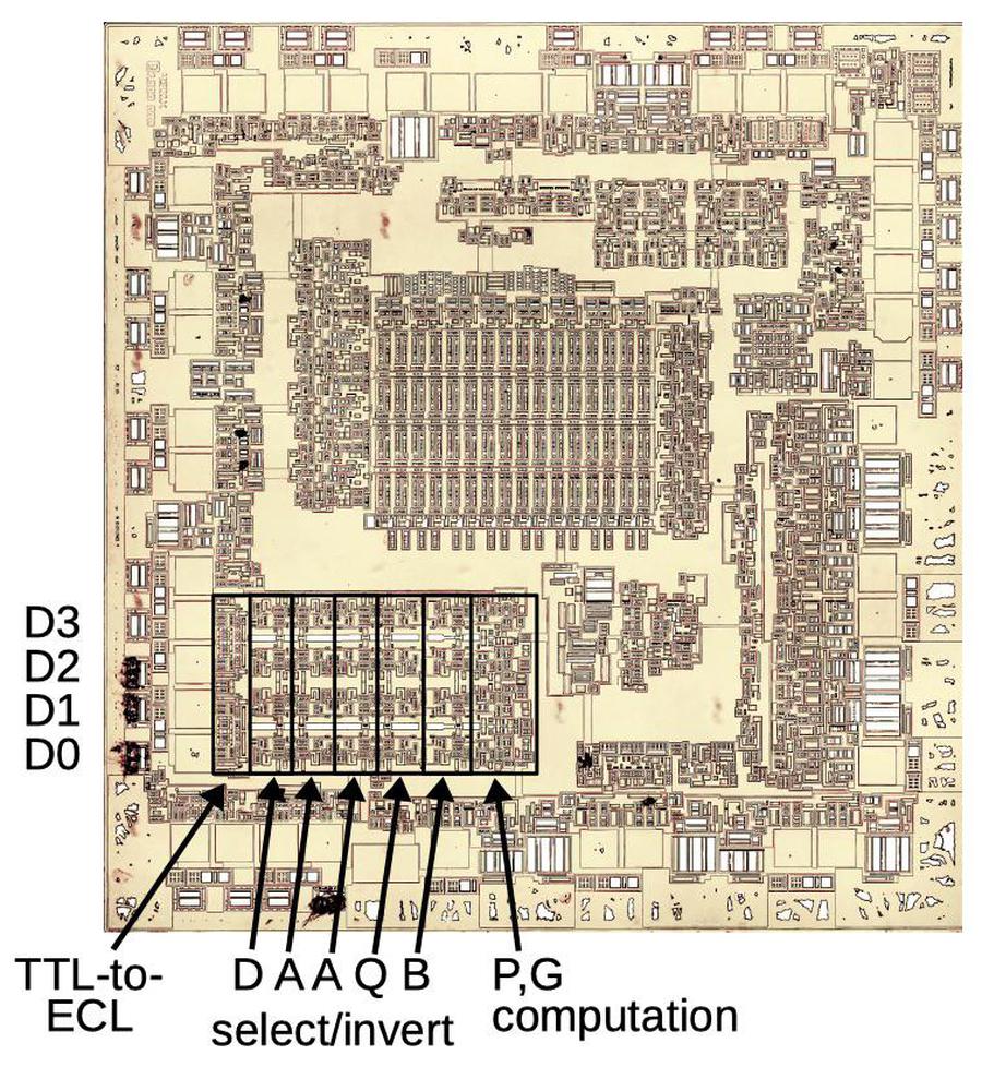
I'll give a brief explanation of the ALU circuitry, starting with the selector. The first two selector boxes below (D and A) select the ALU's first argument, while the last three (A, Q, and B) select the ALU's second argument. Each selector box implements the function Select · (Value ⊕ Invert), where Value is a potential input value, Select is 1 to select that value, and Invert is 1 to invert the value. (Since the ALU is four bits wide, four bits are selected. Each selector box is implemented with four ECL gates; see the footnote for details.13) By enabling one of the Select lines, the desired value is selected. If no Select line is enabled, the value to the ALU is 0.12 Note that the selector can also invert the input; the chip performs subtraction by adding the inverted value.

The first part of the ALU consists of four horizontal layers, one for each bit.

The first part of the ALU consists of four horizontal layers, one for each bit.

Once the two ALU inputs have been selected, the ALU computes "Propagate" (P) and "Generate" (G) bits for each pair of input bits. This is part of the carry lookahead,9 used for high-speed addition.

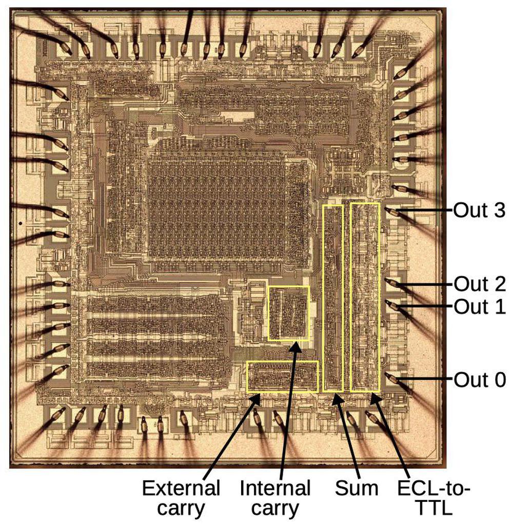
The photo below indicates the remaining parts of the ALU circuitry. (For variety, this die photo shows the metal layer, while the previous showed silicon.) The P and G signals from the previous circuit go to two blocks of carry computation circuitry. The lower carry block computes external P, G, and carry signals that provide carry lookahead across multiple chips; this allows fast addition for larger words.14 The upper carry block computes the carries that are used internally. The "sum" circuitry computes the sum for each bit using the carry, P, and G values. The important thing is that the sum for each bit can be computed in parallel, thanks to the carry lookahead. Finally, the output circuitry converts the internal ECL signals to TTL signals and drives the four output pins.15

The remaining ALU circuitry.

The remaining ALU circuitry.

The chip uses some interesting techniques to reuse the adder hardware for its eight operations. The selector circuit described earlier can optionally complement its input. This is used for subtraction, as well as for some logic functions. To perform logic operations (instead of addition/subtraction), the carry computation is disabled. (For a logic operation, each bit position is unaffected by what happens in other bit positions.) Finally, the adder's EXCLUSIVE OR circuit is turned into AND by forcing the P signals high.16 Thus, instead of using eight different circuits for the ALU's eight operations, the chip uses a single circuit with a few carefully-chosen tweaks. 17

Conclusion

The Am2901C chip is interesting because it is an example of high-speed ECL circuitry, a relatively uncommon logic family. The chip's ALU is spread across the lower half of the chip, implementing eight different functions and using carry lookahead for high performance. Although the chip is complex, it can be reverse-engineered with careful examination under a microscope.

Bit-slice processors such as the Am2901 were used in minicomputers and many other systems in the 1970s and 1980s. Eventually, though, improvements in CMOS technology permitted a fast processor to be implemented on a single chip, rendering the bit-slice processor obsolete. While the Am2901 had maybe a thousand transistors and ran at 16MHz, AMD now makes processors that have billions of transistors and run at 4GHz.

Follow me @kenshirriff for more reverse engineering. I also have an RSS feed.

Notes and References

  1. Microprocessors on a single chip existed at the time, but they used MOS transistors that were slower than the bipolar transistors used in most minicomputers. They also generally had smaller word sizes. Eventually, CMOS processors became faster than bipolar processors; CMOS is what almost all computers now use. 

  2. The Atari Battlezone documentation (p40) doesn't refer to the Am2901 explicitly, but gives it the Atari part number 137004-001 and calls it a "Transistor Array". Moreover, the schematic (p9) obfuscates the Am2901 pinout, showing 20 address pins and 8 data pins, so it looks like a ROM. (In contrast, all the 7400-series chips are described accurately.) Perhaps Atari was attempting to prevent cloning of the video games by hiding the identity of a few key chips. 

  3. A popular alternative to the Am2901 in many minicomputers was the 74181 ALU chip. This provided arithmetic and logic functions, but not the registers of the Am2901. 

  4. Some complications arise in bit-slice processors, since the slices aren't entirely independent. For instance, when adding two numbers, the carry from one slice needs to be passed into the next slice. Operations such as determining the sign of a number or testing if a number is zero, also require the slices to cooperate. The Am2901 has outputs to support these functions. 

  5. For a detailed discussion of bit-slice processors, see Introduction to designing with the Am2901

  6. Is the Am2901 a microprocessor? In my view, the Am2901 is part of a processor and not a complete microprocessor, but it depends on your definition of a microprocessor. I've written a lot more about these definitions in The surprising story of the first microprocessors. Interestingly, the Soviet Union leaned much more towards bit-slice processors (instead of single-chip microprocessors) than the US. While "microprocessor" usually referred to a single-chip processor in the West, bit-slice and single-chip microprocessors weren't really distinguished in the Soviet Union. (According to "Microcomputing in the Soviet Union and Eastern Europe".) 

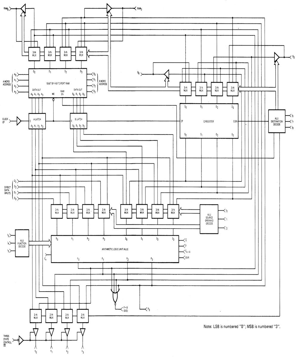
  7. A full block diagram of the Am201 is below. (Click this or any other image for a larger version.) Note that the multiplexers above the RAM and the Q register implement a 1-bit left shift or right shift; they are labeled as "shifters" on the die photo. The multiplexers above the ALU in the block diagram are physically part of the ALU circuitry on the die.

    Block diagram of the Am2901, from the datasheet.

    Block diagram of the Am2901, from the datasheet.


  8. To remove the metal layers from the chip, I alternated applications of Armour Etch to remove the silicon dioxide layer and hydrochloric acid (pool acid) to remove metal. 

  9. Carry lookahead uses "Generate" and "Propagate" signals to determine if each bit position will always generate a carry or will propagate an incoming carry. For instance, if you're adding 0+0+C (where C is the carry-in), there's no way to get a carry out from that addition, regardless of what C is. On the other hand, if you're adding 1+1+C, there will always be a carry out generated, regardless of C. Finally, for 0+1+C (or 1+0+C), there will be a carry out propagated if there is a carry in. Putting this all together, for each bit position you create a G (generate) signal if both bits are 1, and a P (propagate) signal unless both bits are 0, using simple logic gates.

    The formula for computing the carry depends on the bit position. For instance, consider the carry from bit 0 to bit 1. This carry will occur if if P0 is set (i.e. a carry is generated or propagated) and there is either a carry-in or a generated carry. So C1 = P0 AND (Cin OR G0). Higher-order carries have more cases and are progressively more complicated. For example, consider the carry in to bit 2. First, P1 must be set for a carry out from bit 1. As well, a carry either was generated by bit 1 or propagated from bit 0. Finally, the first carry must have come from somewhere: either carry-in, generated from bit 0 or generated from bit 1. Putting this all together produces the function used by the Am2901: C2 = P1 AND (G1 OR P0) AND (C0 OR G0 OR G1). Formulas for the various carries and external P, G, and carry are given in the datasheet, Figure 9. 

  10. ECL gates obtained much of their speed advantage because the transistors were not completely turned on (i.e. saturated). This allowed the transistors to switch the current path rapidly. Additionally, the difference between a "0" voltage and a "1" voltage was small (about 0.8) volts, so signals could switch between the two voltages quickly. In comparison, TTL gates typically had a difference of about 3.2 volts between a "0" and a "1", requiring more time to switch. (Signals could typically switch at about 1 volt per nanosecond, so a larger voltage swing caused nanoseconds of delay.) On the other hand, the small voltage swings of ECL made the circuits more sensitive to electrical noise. 

  11. The current sink at the bottom of the ECL gate provides an essentially-constant current, controlled by the input voltage VCS. This is an improvement over a simple resistor, since the current through the resistor varies based on the voltage across it, which depends on the input voltages. The current sink circuit also saves space by using a smaller resistor. 

  12. The outputs of the ALU select gates are connected together with a wired-OR. The unselected values output 0, so the value on the wire is the desired one. In this way, the circuit implements a multiplexer with minimal circuit. 

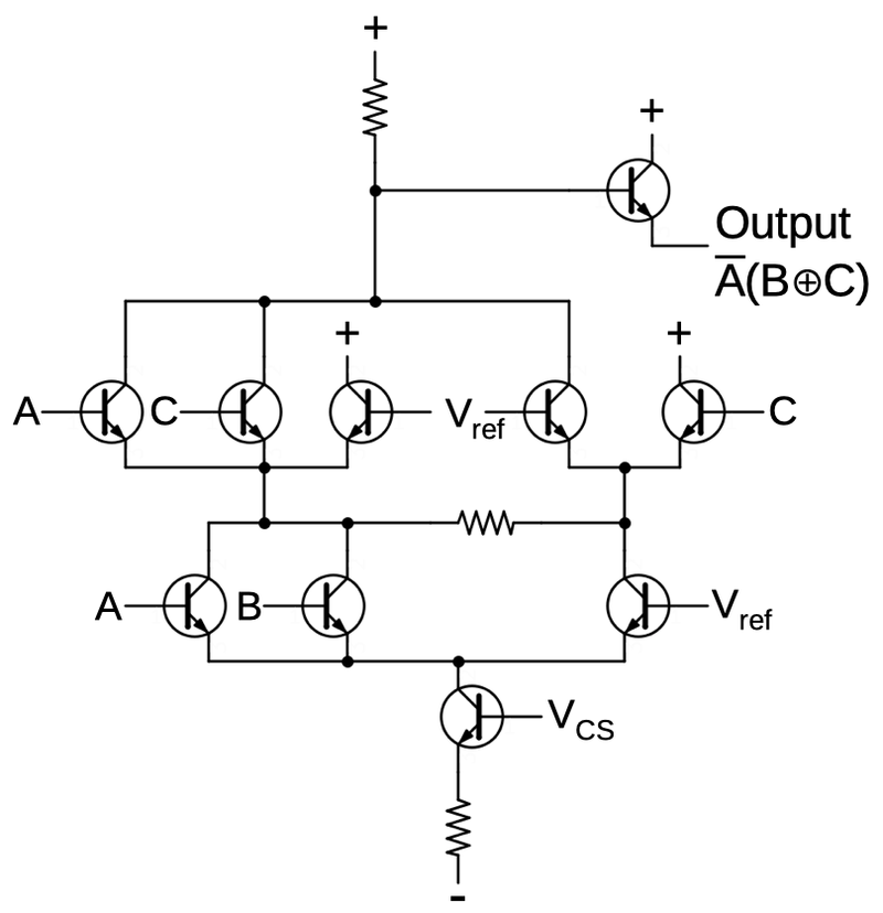
  13. The diagram below shows the AND-XOR circuit used in the AM2901 ALU that implements A' · (B ⊕ C). I'll briefly explain its operation. If input A is high, current flows through the leftmost transistors, pulling the output low. If B and C are both high, current through the left B and C transistors pulls the output low. If B and C are both low, current through the Vref transistors pulls the output low. If B and C are different, the current is sourced from on the "+" transistors so the output remains high. The key point is that a single ECL gate can implement a complex function; in contrast, XOR is difficult with most logic families. (I find ECL logic reminiscent of 1920s-era relay logic because it switches between two paths, rather than switching on or off.)

    Schematic of an ECL AND-XOR circuit. It is slightly simplified: the input voltage levels for the lower half need to be a diode drop lower than the upper inputs. I'm not sure of the purpose of the horizontal resistor.

    Schematic of an ECL AND-XOR circuit. It is slightly simplified: the input voltage levels for the lower half need to be a diode drop lower than the upper inputs. I'm not sure of the purpose of the horizontal resistor.

    The only reference I've found for complex ECL circuits is The VLSI Handbook chapter 38. 

  14. The carry lookahead techniques can be implemented across multiple chips for fast additions larger than 4 bits. Each chip generates a Generate and Propagate signal, indicating if that chip will generate a carry or propagate a carry-in. These signals are combined by a look-ahead carry generator chip such as the Am2902 look-ahead carry generator chip

  15. The output circuitry also includes multiplexers; the chip can either output the ALU result or the A register value. 

  16. The chip uses the P and G values to generate the sum of inputs R and S with carry-in C. The sum is (R ⊕ S ⊕ C)', computed as ((P' ∨ G) ⊕ C)', where P = R∨S and G = R•S. If P is forced to 1, (P' ∨ G) reduces to G, which is R•S. Thus, by changing P, the same circuit can be used to compute the AND of the inputs R and S. 

  17. The table below shows the eight operations that the ALU can compute. Three of the instruction bits fed into the chip are used to select the operation: I5, I4, and I3. The "Function" column in the table shows the function as documented, while the "Computation" column shows how each bit of the function is computed internally. First, note that the operations all boil down to EXCLUSIVE OR (⊕) or AND (∧). Addition is performed by bitwise EXCLUSIVE OR of the two arguments and the carry bits. Subtraction is performed by complementing an argument and then adding. For example, adding the complement of R (R') is the same as subtracting R. Bit I3 complements R, while bit I4 complements S. Note that the EXCLUSIVE OR operations (EXOR and EXNOR) use the same circuitry as addition, but carry computation is blocked. The AND operation is performed by blocking the G signal. Finally, OR is computed using De Morgan's law, which shows that R' ∧ S' = (R ∨ S)'. The point of this is that the Am2901 doesn't need separate circuitry for addition, subtraction, AND, OR, and EXCLUSIVE OR, but reuses most of the circuitry.

    MnemonicI5I4I3FunctionComputation
    ADD000R Plus SR ⊕ S ⊕ Carry
    SUBR001S Minus RR' ⊕ S ⊕ Carry
    SUBS010R Minus SR ⊕ S' ⊕ Carry
    OR011R OR S(R' ∧ S') ⊕ 1
    AND100R AND SR ∧ S
    NOTRS101R' AND SR' ∧ S
    EXOR110R EX OR SR ⊕ S' ⊕ 1
    EXNOR111R EX NOR SR' ⊕ S' ⊕ 1
     

A circuit board from the Saturn V rocket, reverse-engineered and explained

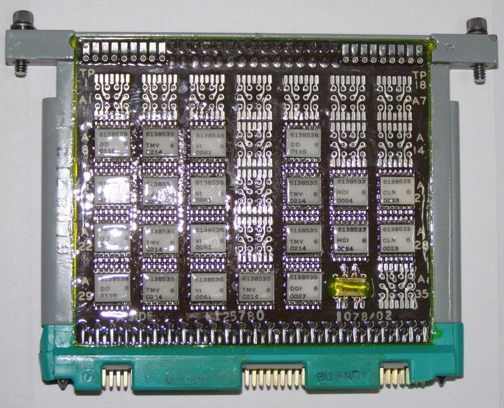
In the Apollo Moon missions, the Saturn V rocket was guided by an advanced onboard computer system built by IBM. This system was built from hybrid modules, similar to integrated circuits but containing individual components. I reverse-engineered a circuit board from this system and determined its function: Inside the computer's I/O unit, the board selected different data sources for the computer.

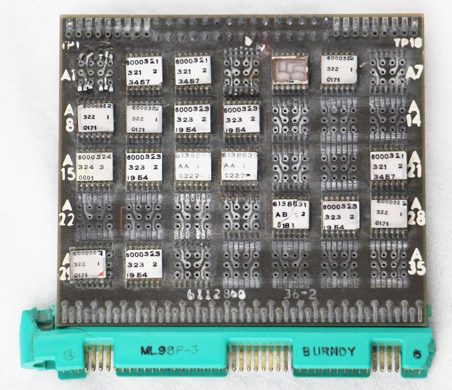
A circuit board from the Saturn V LVDA. (Click this image (or any others) for a larger version.) This board was partially disassembled when I received it and some chips are missing.

A circuit board from the Saturn V LVDA. (Click this image (or any others) for a larger version.) This board was partially disassembled when I received it and some chips are missing.

This post explains how the board worked, from the tiny silicon dies inside its hybrid modules to the board's circuitry and its wiring in the rocket. This board was first studied by Fran Blanch in The Apollo Saturn V LVDC Project. Then EEVblog made a video about it. Now it's my turn to analyze the board.

The Launch Vehicle Digital Computer (LVDC) and Launch Vehicle Data Adapter (LVDA)

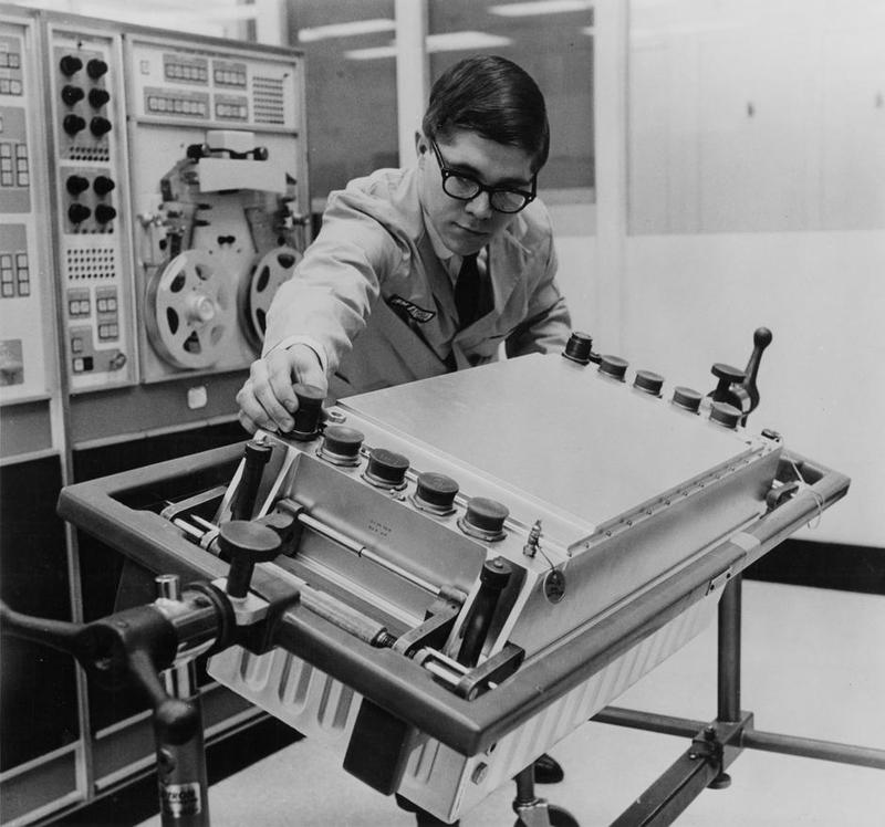
The race to the Moon started on May 25, 1961, when President Kennedy stated that America would land a man on the Moon before the end of the decade. This mission required the three-stage Saturn V rocket, the most powerful rocket ever built. The Saturn V was guided and controlled by the Launch Vehicle Digital Computer (below), from liftoff into Earth orbit, and then on a trajectory towards the Moon.1 In an era when most computers ranged from refrigerator-sized to room-filling, the LVDC was very compact and weighed just 80 pounds since it was mounted inside the rocket. The downside was that it was very slow, performing 12,000 instructions a second.

The LVDC mounted in a support frame for testing. Behind the operator is a test system called ACME (Aerospace Computer Manual Exerciser). The ACME paper tape reader is visible at the back. Photo from IBM.

The LVDC mounted in a support frame for testing. Behind the operator is a test system called ACME (Aerospace Computer Manual Exerciser). The ACME paper tape reader is visible at the back. Photo from IBM.

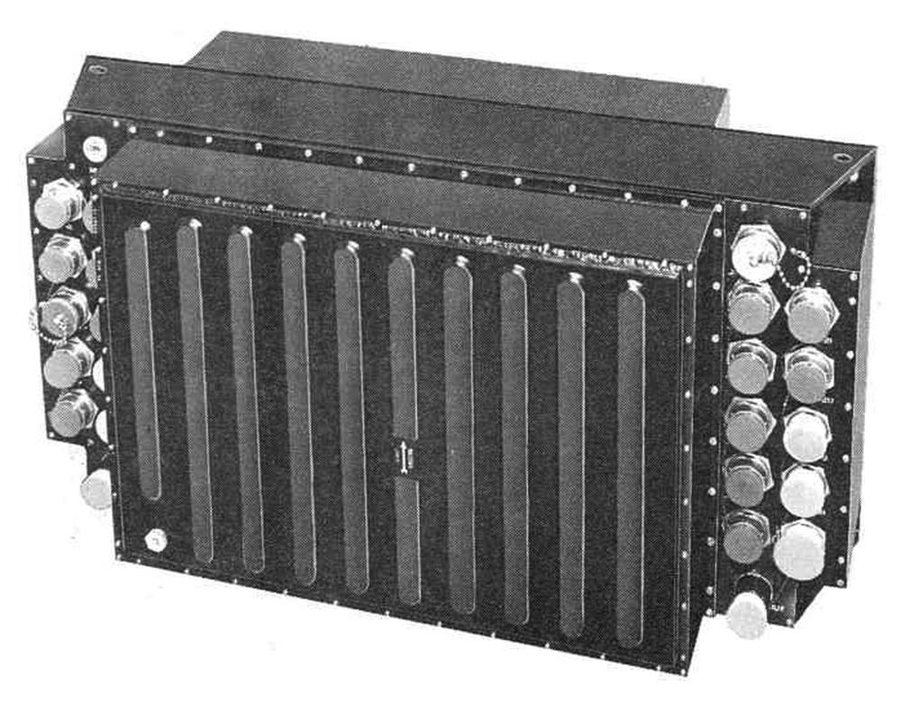
The LVDC worked in conjunction with the Launch Vehicle Data Adapter (LVDA, below), which provided the input/output functions for the computer. All communication between the computer and the rocket went through the LVDA, which converted the rocket's analog signals and 28-volt control signals to the serial binary data the computer required. The LVDA contained buffers (implemented with glass delay lines) and control registers for its various functions. The LVDA had analog-to-digital converters to read data from the inertial measurement unit's gyroscopes and digital-to-analog converters to provide control signals to the rockets. It also processed telemetry signals that were sent to the ground and received ground-based commands for the computer. Finally, power to the LVDC was provided by redundant switching power supplies in the LVDA.

The Saturn V LVDA was a 176-pound box that provided I/O for the LVDA. It had 21 round connectors for cables to other parts of the rocket.  From System Description and Component Data.

The Saturn V LVDA was a 176-pound box that provided I/O for the LVDA. It had 21 round connectors for cables to other parts of the rocket. From System Description and Component Data.

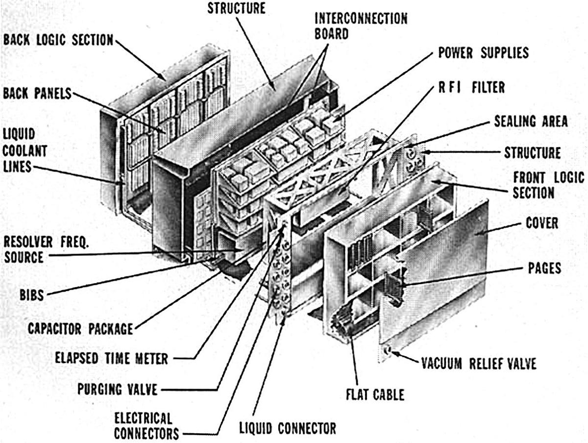
Because the LVDA had so many different functions, it was almost twice the size of the LVDC computer. The diagram below shows the circuitry crammed into the 176-pound LVDA.2 It had two sections filled with circuit boards called "pages": the front logic section and the back logic section. (The board I examined was from the front logic section.) The power supplies and filters were in the central section. A methanol coolant solution flowed through channels in the LVDA to keep it cool. The LVDA was wired to the LVDC and other parts of the rocket through the 21 round connectors on the ends.

Exploded diagram of the LVDA, from NASA.

Exploded diagram of the LVDA, from NASA.

Diode-Transistor Logic

There are many different ways to build logic gates. The LVDC and LVDA used a technique called Diode-Transistor Logic (DTL) that builds a gate from diodes and a transistor. This was more advanced than the Resistor-Transistor Logic (RTL) used by the Apollo Guidance Computer, but inferior to Transistor-Transistor Logic (TTL), which became very popular in the 1970s.

The standard logic gate in the LVDC was an AND-OR-INVERT gate3 that implements a logic function such as (A·B + C·D)'. It gets its name because it ANDs together sets of inputs, ORs them, and finally inverts the results. The AND-OR-INVERT gate was powerful because it could be built with many inputs, e.g. (A·B + C·D·E + F·G·H)'. While the AND-OR-INVERT gate may seem complex, it only required one transistor which was important in an era when every transistor counted.

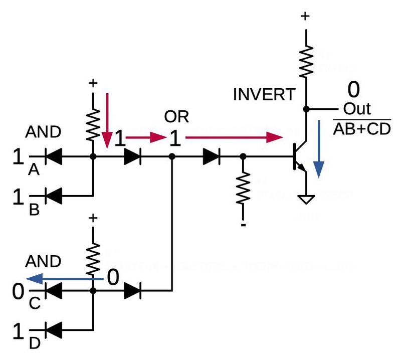
If you want to understand how the gate works internally, look at the diagram below. It shows a four-input AND-OR-INVERT gate with two AND terms. First consider inputs A and B, which are both set to 1 (high). The pull-up resistor4 pulls the AND value high (red, 1). In comparison, in the lower AND gate, input C is 0, so current flows through input C, pulling the AND value low (blue, 0). Thus, the diodes and the pull-up resistor implement an AND gate. Next, look at the OR stage. Current from the top AND (red) pulls the OR stage high (1). Finally, this current turns the transistor on, pulling the output low (blue, 0) and providing the inversion. If both AND stages were 0, the OR stage wouldn't be pulled high. Instead, the pull-down resistor would pull the OR value low (0), turning off the transistor and causing the output to be pulled high (1).

An AND-OR-INVERT gate computing (A·B + C·D)'. Since inputs A and B are both high, the output is pulled low.

An AND-OR-INVERT gate computing (A·B + C·D)'. Since inputs A and B are both high, the output is pulled low.

An AND-OR-INVERT gate could be built with more resistors or diodes to provide as many inputs as required, potentially many inputs to each AND, and many blocks ORed together. You might expect that AND-OR-INVERT gate would be implemented on a single chip, but the LVDC used multiple chips for each gate, as will be shown below. Different chips had various combinations of diodes, resistors, and transistors that were wired up in flexible ways to form the desired logic gate.

Unit Logic Devices (ULD)

The LVDC and LVDA were built with an interesting hybrid technology called ULD (Unit Logic Devices).5 Although they superficially resembled integrated circuits, ULD modules contained multiple components. They used simple silicon dies, each implementing just one transistor or two diodes. These dies, along with thick-film printed resistors, were mounted on a .3-inch-square ceramic wafer. These modules were a variant of the SLT (Solid Logic Technology) modules used in IBM's popular S/360 series of computers. IBM started developing SLT modules in 1961, before integrated circuits were commercially viable, and by 1966 IBM produced over 100 million SLT modules a year.

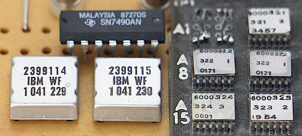
ULD modules were considerably smaller than SLT modules, as shown in the photo below, making them more suitable for a compact space computer. ULD modules used flat-pack ceramic packages instead of SLT's metal cans, and had metal contacts on the upper surface instead of pins. Clips on the circuit board held the ULD module in place and connected with these contacts. The LVDC and LVDA used more than 50 different types of ULDs.

ULD modules (right) are smaller than SLT modules or more modern DIP integrated circuits (left). An SLT module was about 0.5" on a side, while a ULD module was 0.3" on a side and much thinner.

ULD modules (right) are smaller than SLT modules or more modern DIP integrated circuits (left). An SLT module was about 0.5" on a side, while a ULD module was 0.3" on a side and much thinner.

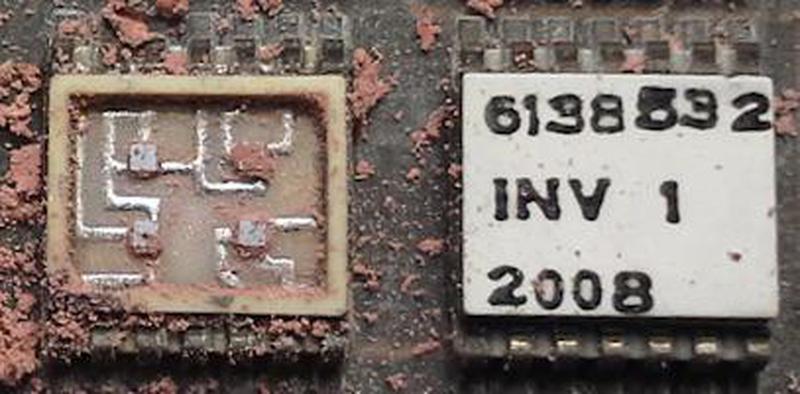
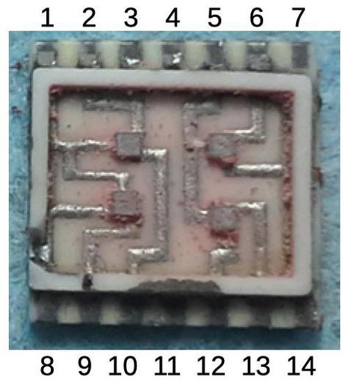
Internally, a ULD module contained up to four tiny square silicon dies. Each die implemented either two diodes or one transistor. The photo below shows the internal components of a ULD module, next to an intact ULD module. On the left, the circuit traces are visible on the ceramic wafer, connected to four tiny square silicon dies. While this looks like a printed circuit board, keep in mind that it is much smaller than a fingernail. Thick-film resistors were printed on the underside of the module, so they are not visible.

A ULD of type "INV" opened to show the four silicon dies inside. The upper-right die is a transistor, while the other three dies are dual diodes. The module was protected by pink silicone, which has been removed to show the circuitry. Photo courtesy of Fran Blanche.

A ULD of type "INV" opened to show the four silicon dies inside. The upper-right die is a transistor, while the other three dies are dual diodes. The module was protected by pink silicone, which has been removed to show the circuitry. Photo courtesy of Fran Blanche.

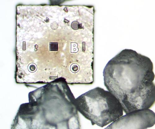
The microscope photo below shows a silicon die from a ULD module that implements two diodes. The die is very small; for comparison, grains of sugar are displayed next to the die. The die had three external connections through copper balls soldered to the three circles. The two lower circles were doped (darker regions) to form the anodes of the two diodes, while the upper circle was the cathode, connected to the substrate. Note that this die is much less complex than even a basic integrated circuit.

Photo of a two-diode silicon die next to sugar crystals. This photo is a composite of top-lighting to show the die details, with back-lighting to show the sugar.

Photo of a two-diode silicon die next to sugar crystals. This photo is a composite of top-lighting to show the die details, with back-lighting to show the sugar.

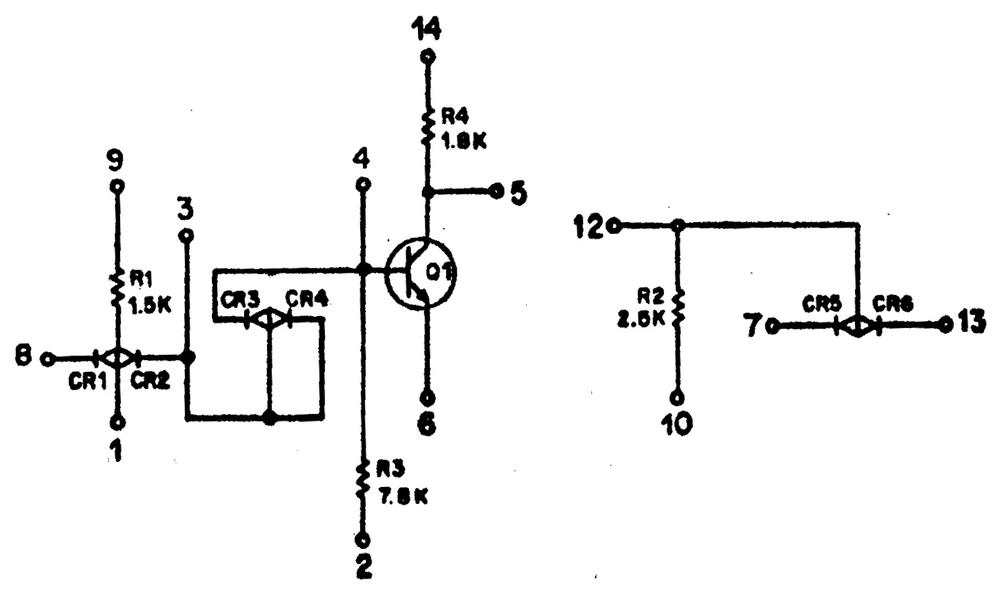
The schematic below shows the circuitry inside the "INV" module shown earlier.7 The left side forms an AND-OR-INVERT gate with a single input. A gate with a single input may seem pointless, but additional AND inputs can be attached to pin 1 and additional OR gates can be attached to pin 3. The right side of the schematic provides components that can be used as additional inputs.
Schematic of the "INV" inverter module. Based on  Saturn V Guidance Computer, Semiannual Progress Report, page 2-37. Pins 7 and 14 switched from original, which didn't match the actual circuitry.

Schematic of the "INV" inverter module. Based on Saturn V Guidance Computer, Semiannual Progress Report, page 2-37. Pins 7 and 14 switched from original, which didn't match the actual circuitry.

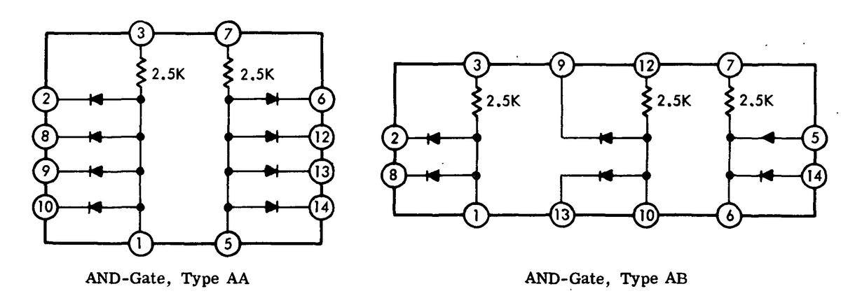
The board also uses AND gate modules (types "AA" and "AB"), shown below. Keep in mind that these aren't independent gates, but components that can be wired to an INV chip to provide more AND or OR inputs.6 These modules can be wired up in many flexible ways; there are no specific inputs and outputs. One common configuration is to use half of an AA chip as a three-input AND gate. Part of an AB chip can provide two more inputs if needed.

Internal schematics of the type "AA" and type "AB" AND gates. From Laboratory Maintenance Instructions for LVDA, Vol 1.

Internal schematics of the type "AA" and type "AB" AND gates. From Laboratory Maintenance Instructions for LVDA, Vol 1.

The photo below shows the semiconductors (dual diodes) inside an AA gate. You can match up the components with the schematic above if you wish; pins 1 and 5, the common pins, are most interesting. Note that the pin numbering does not match the standard IC scheme.

A ULD of type "AA" opened to show the four silicon dies inside. The four dies are dual diodes with the cathodes connected. Original photo courtesy of Fran Blanche.

A ULD of type "AA" opened to show the four silicon dies inside. The four dies are dual diodes with the cathodes connected. Original photo courtesy of Fran Blanche.

The board's circuitry

To determine what the board did, I tediously beeped out the connections between chips with a multimeter to create wiring diagrams. (Shortly after I finished, LVDA manuals with schematics turned up8 making my reverse-engineering effort unnecessary.) The board forms a 7-input multiplexer, selecting one of 7 input lines and storing the value in a latch. With 1960s technology, this simple function required a whole board of chips.

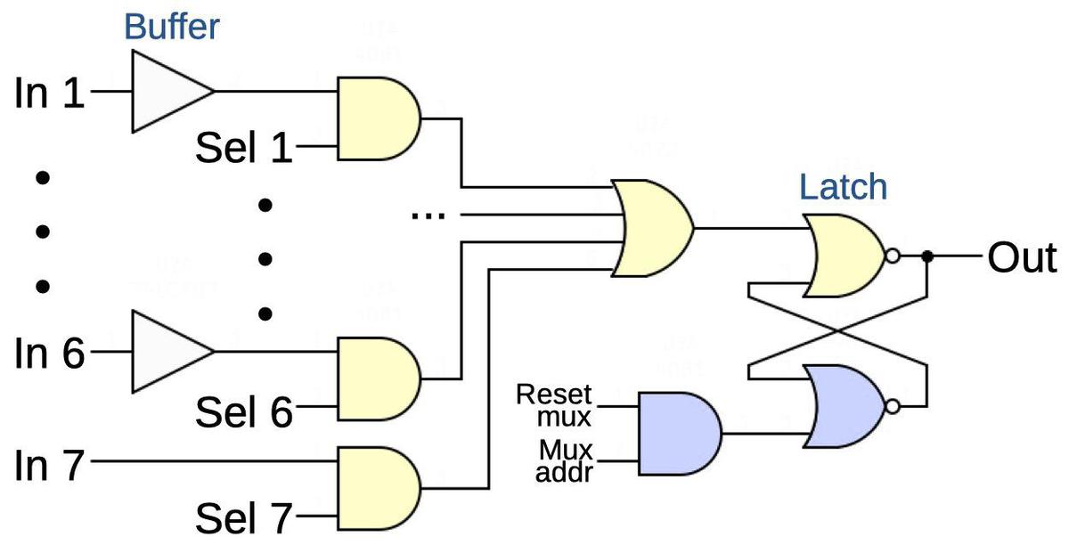
The schematic below is a simplified diagram of the board. At the left, the board receives 7 inputs; six of them are 28-volt signals that need to be buffered to generate logic signals, while the seventh is already a 6-volt logic signal. One of the seven select lines is energized to select the corresponding input, which is then stored in the latch.9 (The main simplification is that there are multiple select lines for each input. The full schematic is in the footnotes.10) When the "reset multiplexer" signal and the "multiplexer address" are energized, the latch is reset.

Simplified schematic of the board. It is a multiplexer that selects one of the six inputs and stores the value in the latch.

Simplified schematic of the board. It is a multiplexer that selects one of the six inputs and stores the value in the latch.

While the schematic shows many logic gates, it is implemented with just two AND-OR-INVERT gates. The yellow gates form one large AND-OR-INVERT gate, while the blue gates form a second. (The two yellow OR gates merge into one.) The two gates are implemented across eight chips: two chips of type INV, four AA, and two AB. This illustrates the flexibility and expandability of the AND-OR-INVERT logic model, but it also shows that circuits use many chips. Note that there are only two transistors in the logic circuit (one in each INV chip); almost all of the logic is implemented with diodes.

The buffer circuitry

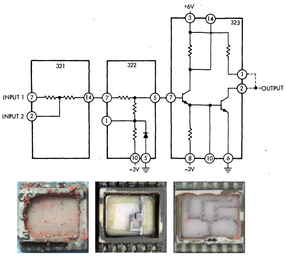
Of the 26 chips on the board, 18 of them were analog chips that buffered and processed the input signals. The inputs were 28-volt signals, while the logic requires 6-volt signals. Each input (except #7) passes through a "Discrete Interface Circuit" that converts the input to a logic signal. The diagram below shows the circuit, built from chips of types 321, 322, and 323.11 The photos show the contents of each chip. Since the 321 chip only consists of resistors (on the underside), the chip appears empty from the top. The 322 chip contains a single diode, while the 323 chip contains two transistors. (The dies are missing from the 323 photo; they are small squares as in the 322.)

Discrete Input Circuit, type A (DIA). The published "322" pinout is wrong, showing two pins 5. From Laboratory Maintenance Instructions for LVDA, Vol 1, Figure A-15.
321 and 322 photos courtesy of Fran Blanche.

Discrete Input Circuit, type A (DIA). The published "322" pinout is wrong, showing two pins 5. From Laboratory Maintenance Instructions for LVDA, Vol 1, Figure A-15. 321 and 322 photos courtesy of Fran Blanche.

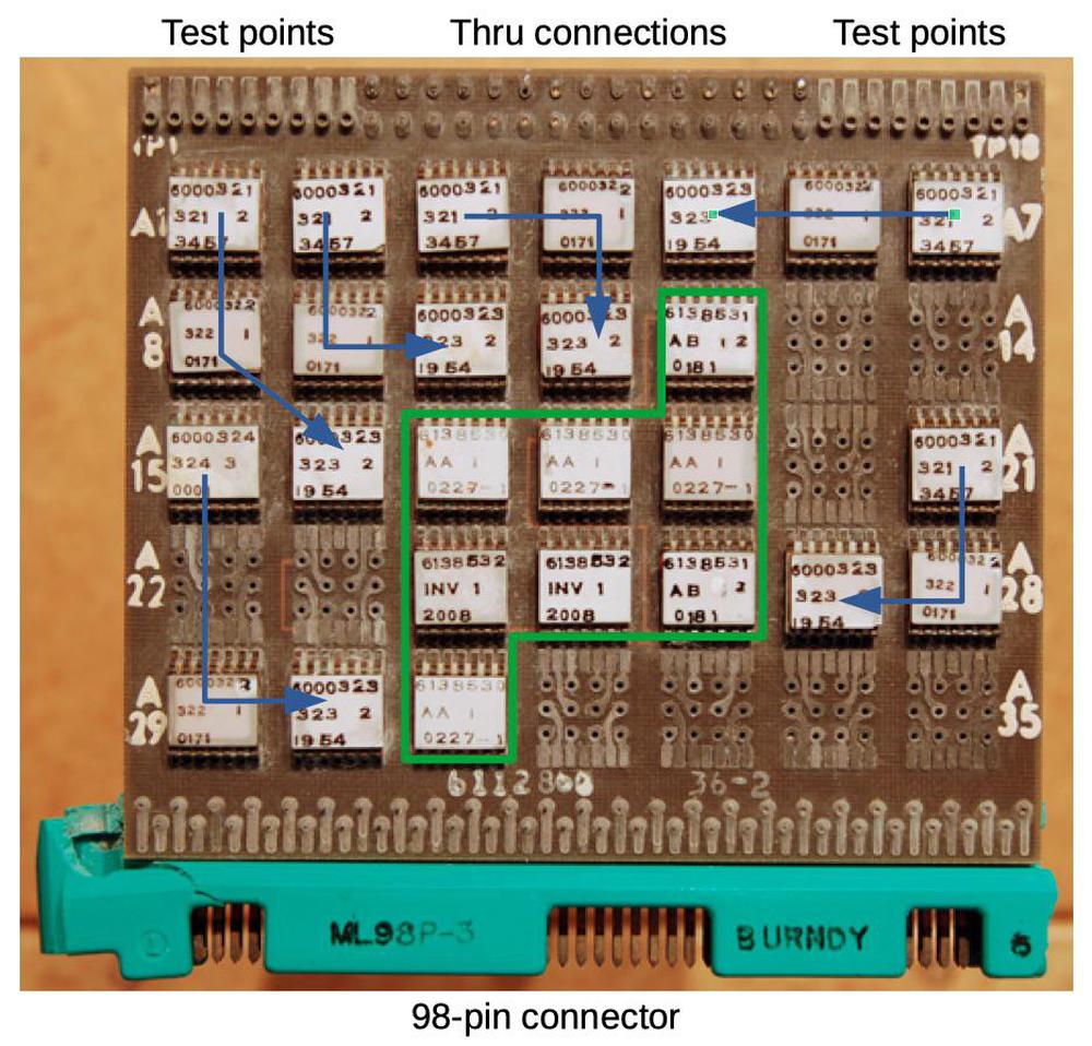
The diagram below summarizes the structure of the board. The eight logic chips in the middle are outlined in green. Each of the six input buffers consists of three chips (321, 322, and 323). The signal flow through these chips is shown with the blue arrows. The board has 35 spots for chips, of which 26 were used. By putting chips in the empty locations, the same circuit board could be reused for slightly different functions.13

The circuit board with input paths in blue and logic circuitry in green. Original photo courtesy of Fran Blanche.

The circuit board with input paths in blue and logic circuitry in green. Original photo courtesy of Fran Blanche.

The board's role in the LVDA

This board was part of the multiplexer in an LVDA subsystem called the "System Data Sampler" that selects signals and sends them either to the computer or to the ground for telemetry. The System Data Sampler consists of a multiplexer that selects one of eight signals, and the Serializer-Selector that converts the 14-bit data to serial form. The multiplexer has several data sources: the RCA-110 ground computer that was connected to the rocket before launch;14 the "command receiver" that received computer commands from the ground after the rocket had launched; the "control distributor" box that provided various discrete signals;12 "spare discrete inputs"; feedback from the "switch selector", a relay box that the computer used to control the rocket; telemetry from the Digital Data Acquisition System (DDAS); and real-time data.

Physically, many of these data sources were large boxes in the Instrument Unit. For instance, the "control distributor" was a 35-pound box next to the LVDA, connected by a thick cable. The LVDA's "command receiver" input came from the "command decoder", a 7.5-pound box connected to other boxes that provided radio input and output. Because the LVDA was cabled to many different devices in the Instrumentation Unit, it required 21 connectors.

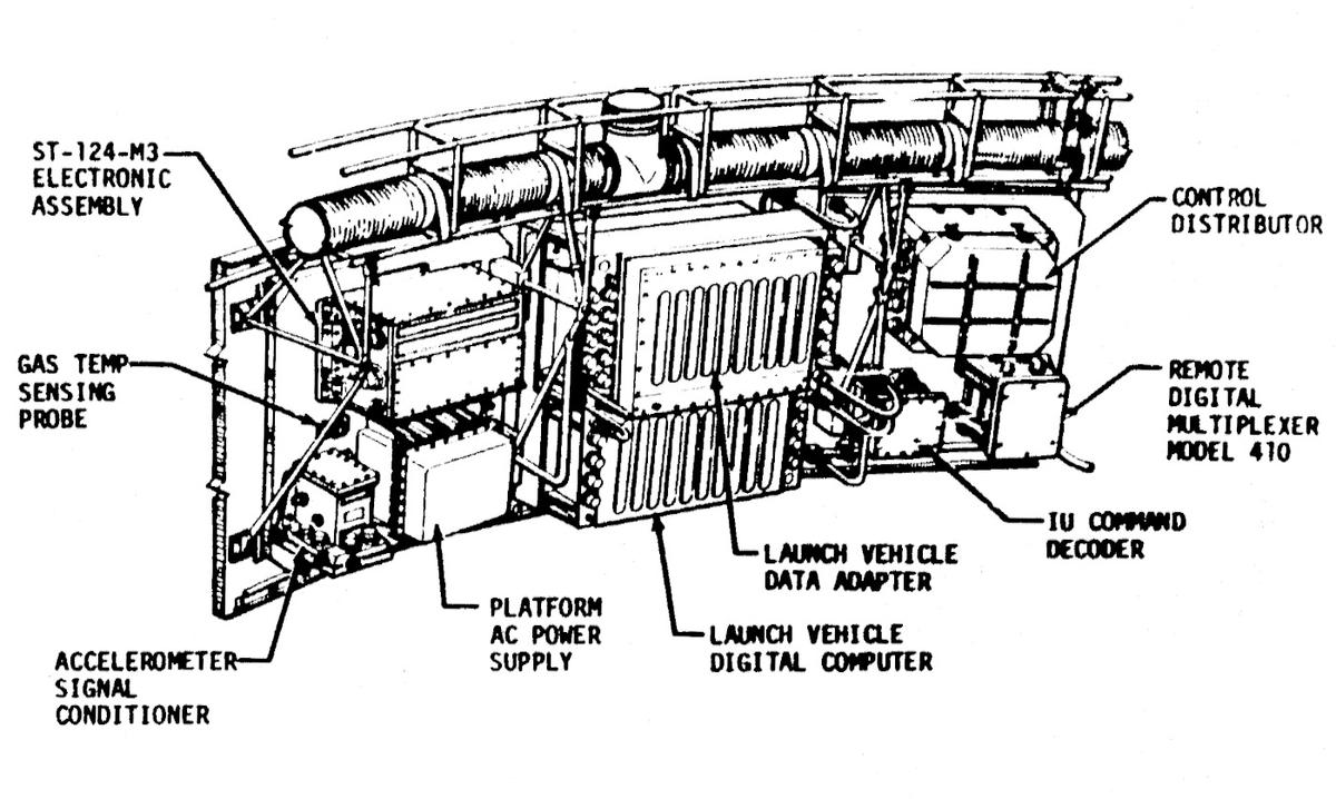
The locations of the LVDA, LVDC, Command Decoder, and Control Distributor in the Instrument Unit. Also shows the electronic assembly (ST-124-M3) that interfaces the inertial measurement unit to the LVDA. From the Saturn V Flight Manual page 7-8.

The locations of the LVDA, LVDC, Command Decoder, and Control Distributor in the Instrument Unit. Also shows the electronic assembly (ST-124-M3) that interfaces the inertial measurement unit to the LVDA. From the Saturn V Flight Manual page 7-8.

The board's physical structure

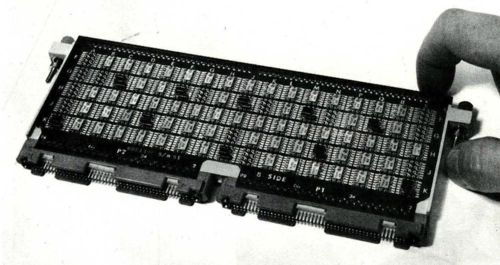
The circuit boards in the LVDA and LVDC used interesting construction techniques to withstand the high accelerations and vibrations of the rocket and to keep the circuitry cool. The board I examined was damaged and missing its mounting frame but the photo below shows an intact unit called a "page". The page's frame is made from a magnesium-lithium alloy that combines light weight, strength, and good heat transfer properties. Heat from a board flowed through the frame to the LVDA or LVDC's chassis, which was liquid-cooled via methanol flowing through channels drilled in the chassis.

A page including the metal frame. This board implemented voting circuitry in the LDVC. Photo from Dmitris Vitoris via Virtual AGC.

A page including the metal frame. This board implemented voting circuitry in the LDVC. Photo from Dmitris Vitoris via Virtual AGC.

Each page could hold two circuit boards, one on the front and one on the back. The printed circuit board has 12 layers, which is a remarkably high number for the 1960s. (Even in the 1970s, commercial PCBs typically had just two layers.) The page has a 98-pin connector, with 49 connections to each PCB. The two boards were connected by 30 "thru pins" at the top of the board. The top of each board also has 18 test connections; these allowed signals to be probed while the boards were installed. (IBM reused this page construction in its System/4 Pi aerospace computers.15)

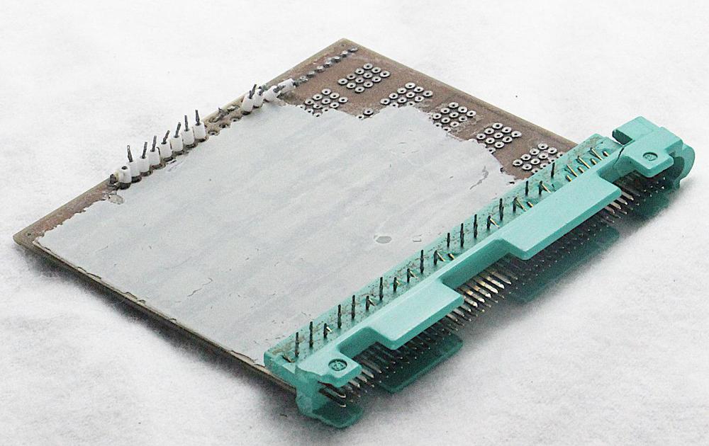
The board I examined had been forcibly separated from the other board in the page. The photo below shows the back of the board. The thru-pins are visible at the top; they would have been connected to the other board. At the bottom, the 49 connections from the connector to the missing board are visible. Some of the board's insulation has been removed, showing the 12 vias at each ULD module position. These provide a connection from a chip pin to any of the 12 layers of the circuit board.

Back of the LVDA board. A second board was mounted on this side originally, but has been removed.

Back of the LVDA board. A second board was mounted on this side originally, but has been removed.

Conclusion

This small circuit board illustrates several stories about computing in the 1960s.

The board used hybrid modules rather than still-new integrated circuits. While this technology may seem backward, it was a key to IBM's success with the IBM System/360 line. Introduced almost exactly 56 years ago (April 7, 1964), these computers used hybrid SLT modules with AND-OR-INVERT logic. These computers dominated the market for years, and the System/360 architecture is still supported by IBM's mainframes.

The LVDC and LVDA also led to IBM's System/4 Pi line of aerospace computers, announced in 1967. These computers used the same "page" design and connectors as this board, even though they abandoned ULD modules for flat-pack TTL integrated circuits. The System/4 Pi line of computers evolved into the AP-101S computers used on the Space Shuttle.

Finally, the board shows the remarkable improvements in technology since the 1960s. Each ULD module contained up to 4 transistors, so even a basic circuit like a multiplexer took a whole board of modules. Now, an iPhone processor has over 8 billion transistors. It's amazing that such simple technology was enough to get to the Moon.

I announce my latest blog posts on Twitter, so follow me @kenshirriff for future articles. I also have an RSS feed. This work builds on Fran Blanche's Apollo Saturn V LVDC Project. Thanks to Fran for providing photos, Ben Krasnow for passing the board along to me, and Mike Stewart for documentation. For more information on the LVDC, see the Virtual AGC project's LVDC page. I recently wrote about the core memory stack in the Saturn V LVDC.

Notes and references

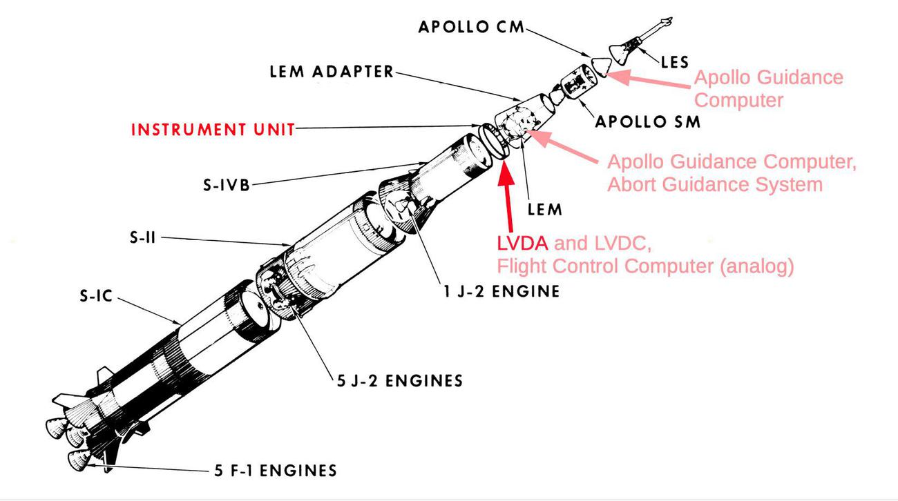
  1. The LVDC was one of several computers onboard the Apollo mission. The better-known Apollo Guidance Computer (AGC) guided the spacecraft to the Moon's surface. (I recently helped restore an Apollo Guidance Computer to running condition.) The Command Module had an AGC while the Lunar Module had a second AGC. The Lunar Module also contained the backup Abort Guidance System computer. The LVDC/LVDA was connected to the Flight Control Computer, a 100-pound analog computer mounted in the Instrument Unit.

    Multiple computers were onboard an Apollo mission. The Launch Vehicle Data Adapter (LVDA) is discussed in this blog post.

    Multiple computers were onboard an Apollo mission. The Launch Vehicle Data Adapter (LVDA) is discussed in this blog post.

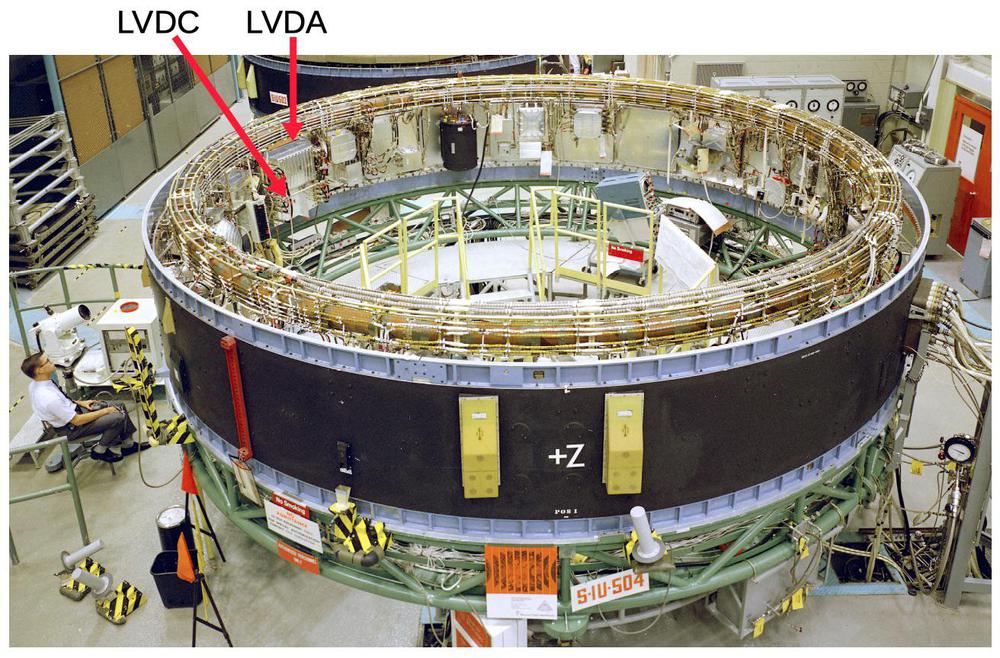
    The LVDA and LVDC were mounted in the rocket's Instrument Unit, a ring between the rocket stages and the payload, the Apollo spacecraft. The Instrument Unit contained the guidance and control systems for the Saturn V rocket as well as extensive telemetry systems sending hundreds of parameters to the ground.

    The Saturn V Instrument Unit under construction. The LVDC (Launch Vehicle Digital Computer) and LVDA (Launch Vehicle Data Adapter) are silver boxes. For scale, note the engineer sitting on the left. Photo from NASA.

    The Saturn V Instrument Unit under construction. The LVDC (Launch Vehicle Digital Computer) and LVDA (Launch Vehicle Data Adapter) are silver boxes. For scale, note the engineer sitting on the left. Photo from NASA.


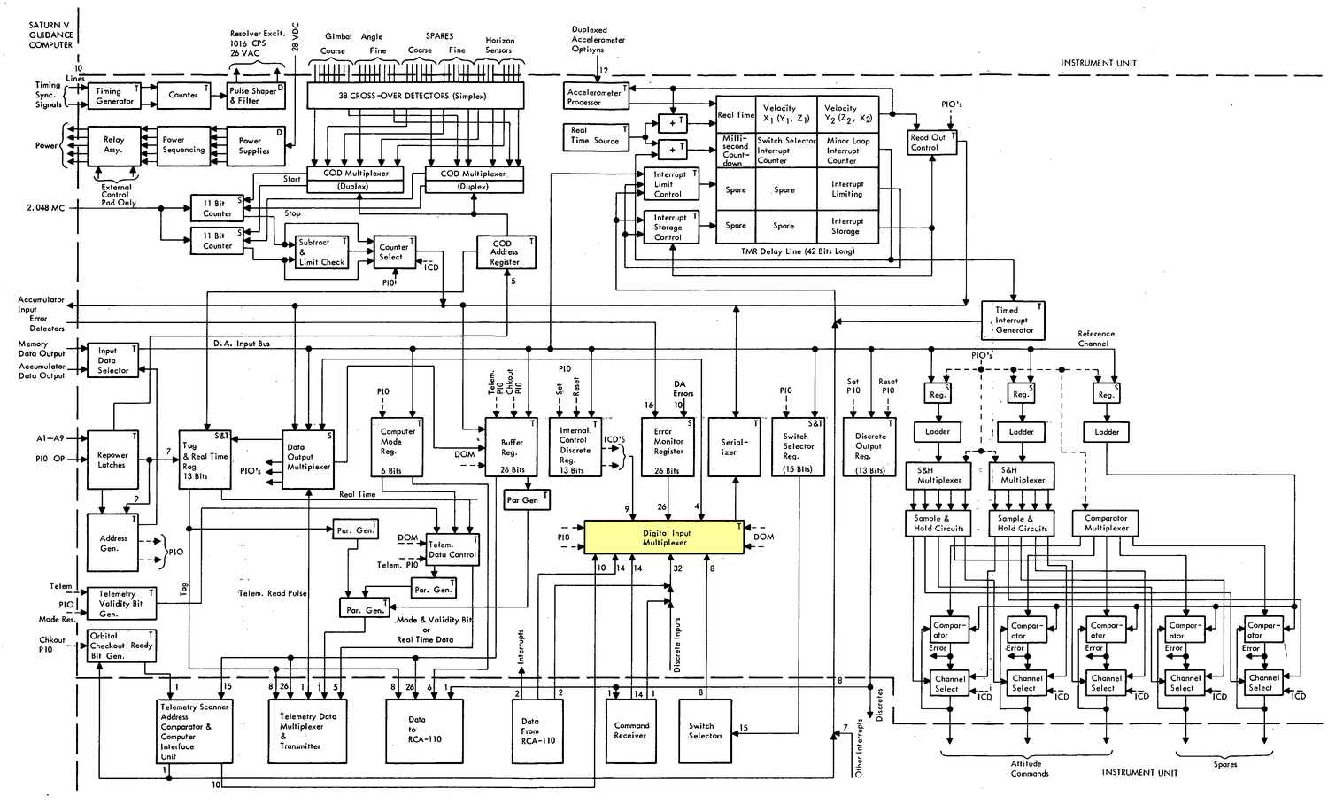
  2. The detailed block diagram of the LVDA below is from the IBM Study Report. (Click the image for a larger version.) This diagram shows that the LVDA has many different functions, registers, and circuits, with many connections to the LVDC (left) and the Instrument Unit (top and bottom). The board I examined is part of the "Digital Input Multiplexer", highlighted in yellow. Note the various data sources feeding into the multiplexer.

    Block diagram from IBM Study Report.

    Block diagram from IBM Study Report.


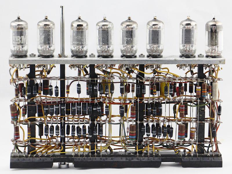
  3. IBM's use of diode-based AND-OR logic goes back to vacuum tube computers from the 1950s. The large 700-series computers primarily used AND-OR diode networks for their logic, with vacuum tubes for amplification instead of transistors. The photo below shows an 8-tube module. Note the large number of diodes (black components with white stripes) in the module below. I think the role of semiconductor diodes is largely ignored in the era of vacuum tube computers. The IBM 709, for instance, used 2000 vacuum tubes and 14,500 diodes in its arithmetic unit.

    Tube module from an IBM 700-series computer in the 1950s. Note the many diodes, especially in the lower left.

    Tube module from an IBM 700-series computer in the 1950s. Note the many diodes, especially in the lower left.


  4. One unusual feature of the LVDC's gates is that the pull-up resistor often isn't connected to the positive voltage source, as you'd expect. Instead, it is connected to a clock signal. When the clock is high, the AND gate functions normally, but when the clock is low, the AND gate is disabled. This has two benefits. First, the pull-up acts as an additional input, ANDing the clock into the result. Second, this reduces power consumption, since there is no current through the pull-up resistor when the clock is low. 

  5. Dr. Wernher von Braun wrote an interesting article about the use of ULD modules for Apollo: Tiny Computers Steer Mightiest Rockets (Popular Science, Oct 1965). 

  6. The ULD logic chips exist in a liminal space, a transition between individual components and integrated circuits. They are not arbitrary components, but neither are they logic gates with defined functions. Instead, they are sets of components that can be pieced together into gates in flexible ways. 

  7. While the ULD chips have 14 pins, the numbering doesn't match normal 14-pin integrated circuits. The top contacts are numbered 1 through 7 (left to right), and the bottom contacts are 8 through 14 (left to right). (Note that The Apollo Saturn V LVDC Project does not use the IBM numbering.) In addition, the circuit board can only use 12 of the pins because of the 12 vias at each position; contacts 4 and 11 (the middle ones) are not connected. 

  8. There is very little documentation available for the LVDC and even less for the LVDA. The Virtual AGC document library is the best source that I found. In particular, the strangely-named "Laboratory Maintenance Instructions for LVDC" volume 1 and volume 2 provide detailed explanations and schematics. The recently-uncovered "Laboratory Maintenance Instructions for LVDA" volume 1 and volume 2 provide similar detail for the LVDA. The System Description and Component Data has photos of the Instrument Unit components and brief descriptions. The Saturn V Flight Manual discusses the LVDC and LVDA at a high level. The IBM Apollo Study Report has more high-level information on the LVDC and LVDA and some nice diagrams. To get more information the LVDC and LVDA, I'll need to visit the US Space and Rocket Center in Huntsville, Alabama, but currently travel is off the table. 

  9. The latch is a circuit to store a single bit; it is a standard SR NOR latch, built by cross-coupling two NOR gates. 

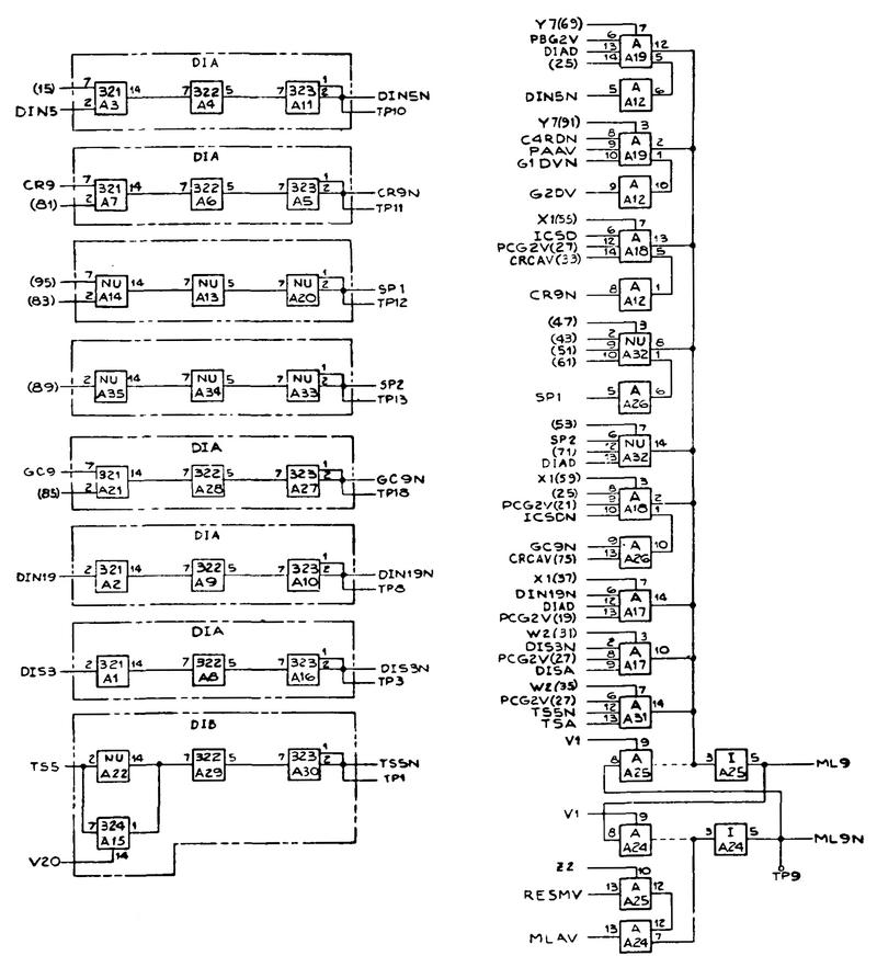
  10. The schematic for the board is below. (Click for full-size.) Each box corresponds to a logic element, part of a chip. The top line "A", "I" shows the element type (AND, INVERT) while the bottom line ("A31") shows the chip position on the board. ("NU" indicates "Not Used"; the board is wired with the circuitry but the chip is not installed.) The left side of the schematic is the input buffers, while the right side is the logic.

    Schematic of the board. From Laboratory Maintenance Instructions for LVDA, Volume II, page 10-114.

    Schematic of the board. From Laboratory Maintenance Instructions for LVDA, Volume II, page 10-114.


  11. Most of the chips in the LVDA/LVDC have descriptive alphabetic codes such as INV (invert), DLD (delay line driver), or ED (error detector). However, the analog chips on the board have numbers instead: 321, 322, 323, and 324. It looks like instead of coming up with descriptive names for these chips, they just took the last three digits of the part number, e.g. "323" has part number "6000323". I also noticed that on the 6000322 parts, the last "2" has been retouched on the chips; I'm not sure what significance that has. 

  12. The "discretes", the binary inputs to the LVDA/LVDC, consisted of high-level signals such as "Liftoff", "S-IB Outboard Engine Out", "S-IVB Engine Manual Cutoff", or "S-IB Stage Separation". I was surprised that the hundreds of measurements throughout the rocket are ignored by the computer; it only cares about the major state transitions such as the engine stopping and a stage separating. (As well as the inertial guidance data, which was key to the computer's navigation.) 

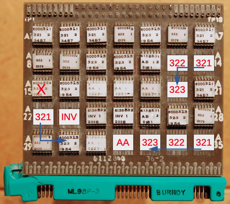
  13. The board has nine empty positions where modules aren't installed, but these positions are wired into the circuitry. The purpose of this is that the same circuit board can be used for multiple functions based on which chips are installed. Specifically, the multiplexer used 13 boards of which 4 were identical to the one I examined, 8 had a few different chips, and 1 was entirely different. The reason for this is that the multiplexer was 14 bits wide, while the inputs were of varying widths. For instance, there were 8 Discrete Input Spares and 10 Telemetry Scanner bits. Thus, some of the boards didn't use some of the inputs and those chips could be omitted, saving a small amount of weight and cost. The diagram below shows the missing chips that can be added.13

    The circuit board with the missing chips filled in. The chip with an X could be replaced by the 321 below it. Original photo courtesy of Fran Blanche.

    The circuit board with the missing chips filled in. The chip with an X could be replaced by the 321 below it. Original photo courtesy of Fran Blanche.

    The board had two unused inputs; to use these, additional 321/322/323 chips were installed. The board also had one input wired up so it could use either a 324 input chip (as in the board I examined) or a 321 input chip. The 321 chip was used for a discrete input that used standard 28-volt signaling, while the 324 chip was used for a signal that was either grounded or floating. The 324 chip included a diode and pull-up resistors. By putting the necessary chip in the appropriate spot, the same PCB could be used for either type of input.

    Two of the boards included an extra logic gate separate from the multiplexer (the INV and AA chips). These gates generated the signals to switch the command input between the RCA-110 mainframe when on the ground, and the radio command decoder after liftoff. In other words, when the umbilical cable pulled out of the Instrument Unit during launch, the signal ("ICS") from the ground computer was lost. Through these two gates, the multiplexer switched the command input from the ground computer to the command decoder, enabling radio commands for the LVDC. 

  14. The RCA-110A computer that communicated with the rocket was in the mobile launch platform, complete with card reader, keypunch, and line printer. In other words, they were moving a whole computer room on the crawler out to the launch pad, with the rocket mounted on top. (In the photo below, the computer room is at the front left of the blue launch platform, under the launcher-umbilical tower.) It communicated with a second RCA-110A computer in the firing room. For details on the mobile launcher and swing arms, see Apollo Maniacs or the book Rocket Ranch. To summarize the wiring, cables went from the RCA-110A computer room near the rocket nozzles, up the tower and across swing arm 7, through the umbilical panel, and to the LVDA. One bit of these signals went to the multiplexer board I examined.

    Apollo 11 Saturn V on the mobile platform, July 1, 1969. Swing arm #7 (marked with arrow) is connected to the Instrument Unit and the top of the S-IVB stage. Photo from NASA.

    Apollo 11 Saturn V on the mobile platform, July 1, 1969. Swing arm #7 (marked with arrow) is connected to the Instrument Unit and the top of the S-IVB stage. Photo from NASA.


  15. IBM's 4 Pi series aerospace computers in the 1960s used the same mechanical board structure as the LVDC, with two multi-layer boards mounted on a "page" mounted in a metal frame. The 4 Pi boards were also double-width or triple-wide compared to the LVDC boards, using two or three of the same 98-pin connections. (Compare the board below with the board that I examined.) The circuitry was entirely different though; the 4 Pi boards used flat-pack TTL integrated circuits instead of ULD modules. The 4 Pi architectures and instruction sets were also entirely different from the LVDC. These early 4 Pi systems were used in aircraft such as the A-7E, F-111 and space missions such as Skylab. The 4 Pi series led to the AP-101 computer used on the Space Shuttle.

    An IBM 4 Pi page. From Technical Description of IBM System 4 Pi Computers (1967).