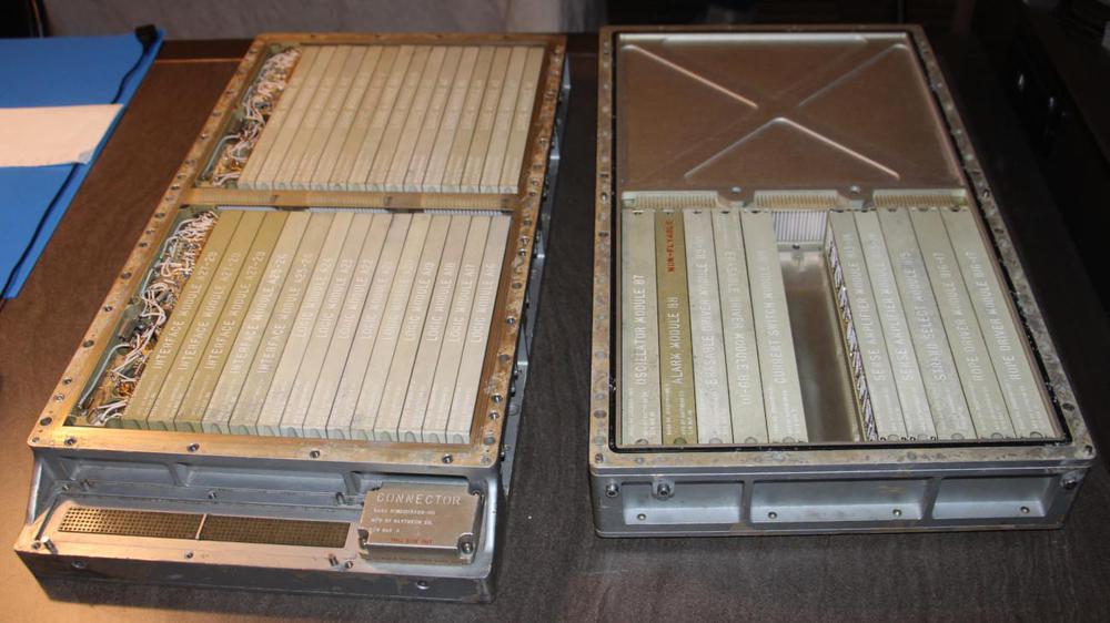
We recently restored an Apollo Guidance Computer1, the computer that provided guidance, navigation, and control onboard the Apollo flights to the Moon. This historic computer was one of the first to use integrated circuits and its CPU was built entirely from NOR gates.2 In this blog post, I describe the architecture and circuitry of the CPU.
Architecture of the Apollo Guidance Computer
The Apollo Guidance Computer was developed in the 1960s for the Apollo missions to the Moon. In an era when most computers ranged from refrigerator-sized to room-sized, the Apollo Guidance Computer was unusual—small enough to fit onboard the Apollo spacecraft, weighing 70 pounds and under a cubic foot in size.
The AGC is a 15-bit computer. It may seem bizarre to have a word size that isn't a power of two, but in the 1960s before bytes became popular, computers used a wide variety of word sizes. In the case of the AGC, 15 bits provided sufficient accuracy to land on the moon (using double- and triple-precision values as needed), so 16 bits would have increased the size and weight of the computer unnecessarily.4
The Apollo Guidance Computer has a fairly basic architecture, even by 1960s standards. Although it was built in the era of complex, powerful mainframes, the Apollo Guidance Computer had limited performance; it is more similar to an early microprocessor in power and architecture.3 The AGC's strengths were its compact size and extensive real-time I/O capability. (I'll discuss I/O in another article.)5
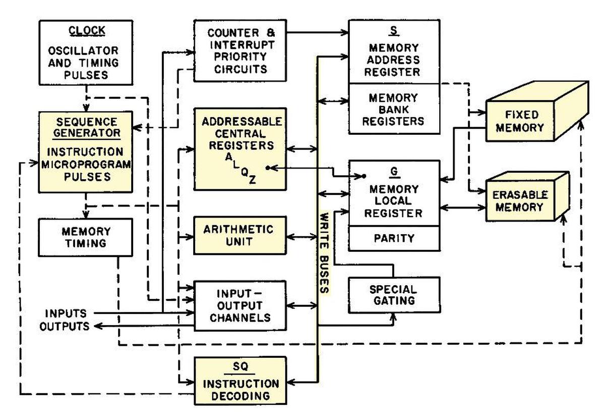
The architecture diagram below shows the main components of the AGC. The parts I'll focus on are highlighted. The AGC has a small set of registers, along with a simple arithmetic unit that only does addition. It has just 36K words of ROM (fixed memory) and 2K words of RAM (erasable memory). The "write bus" was the main communication path between the components. Instruction decoding and the sequence generator produced the control pulses that directed the AGC.
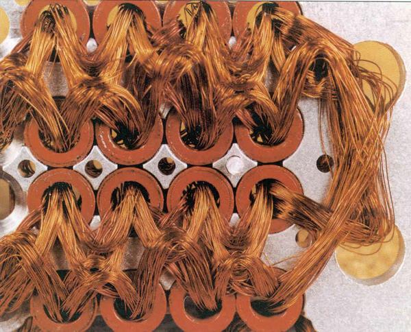
About half of the architecture diagram is taken up by memory, reflecting that in many ways the architecture of the Apollo Guidance Computer was designed around its memory. Like most computers of the 1960s, the AGC used core memory, storing each bit in a tiny ferrite ring (core) threaded onto a grid of wires. (Because a separate physical core was required for every bit, core memory capacity was drastically smaller than modern semiconductor memory.) A property of core memory was that reading a word from memory erased that word, so a value had to be written back to memory after each access. The AGC also had fixed (ROM), the famous core ropes used for program storage where bits were physically woven into the wiring pattern (below). (I've written about the AGC's core memory and core rope memory in detail.)
NOR gates
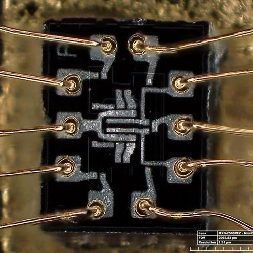
The Apollo Guidance Computer was one of the very first computers to use integrated circuits. These early ICs were very limited; the AGC's chips (below)2 contained just six transistors and eight resistors, implementing two 3-input NOR gates.
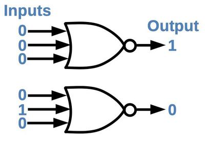
The symbol for a NOR gate is shown below. It is a very simple logic gate: if all inputs are low, the output is high. It might be surprising that NOR gates are sufficient to build a computer, but NOR is a universal gate: you can make any other logic gate out of NOR gates. For instance, wiring the inputs of a NOR gate together forms an inverter. Putting an inverter on the output of a NOR gate produces an OR gate. Putting inverters on the inputs of a NOR gate produces an AND gate.6 More complex circuits, such as flip flops, adders, and counters can be built from these gates.
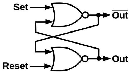
One building block that appears frequently in the AGC is the set-reset latch. This simple circuit is built from two NOR gates and stores one bit of data: the set input stores a 1 bit and the reset input stores a 0 bit. In more detail, a 1 pulse on the set input turns the top NOR gate off and the bottom one on, so the output is a 1. A 1 pulse on the reset input does the opposite so the output is a 0. If both inputs are 0, the latch remembers its previous state, providing storage. The next section will show how the latch circuit is used to build registers.
The registers
The Apollo Guidance Computer has a small set of registers to store values temporarily outside of core memory. The main register is the accumulator (A), which is used in many arithmetic operations. The AGC also has a program counter register (Z), arithmetic unit registers (X and Y), a buffer register (B), return address register (Q)7, and a few others. For memory accesses, the AGC has a memory address register (S) and a memory buffer register (G) for data. The AGC also has some registers that reside in core memory, such as I/O counters.
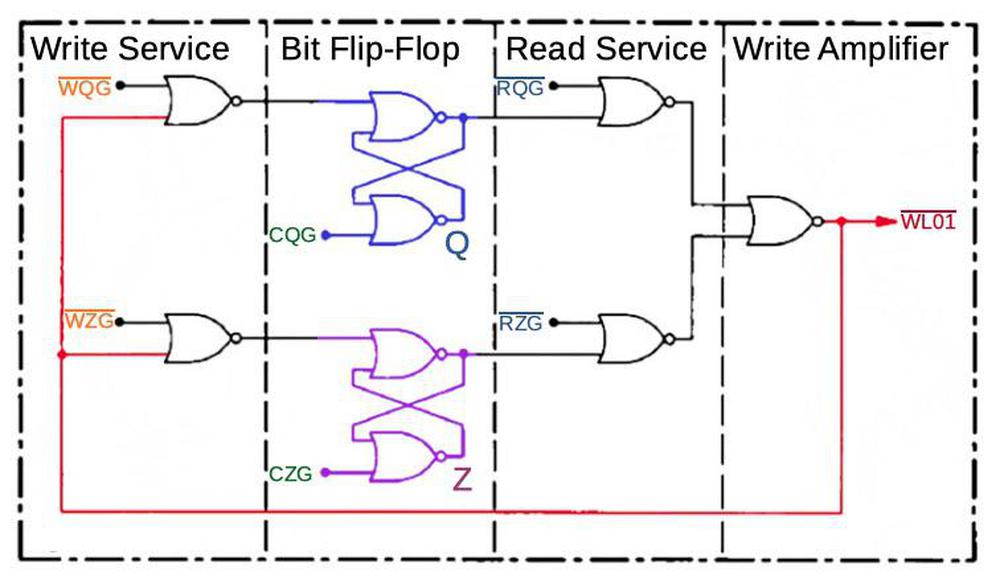
The following diagram outlines the register circuitry for the AGC, simplified to a single bit and two registers (Q and Z). Each register bit has a latch (flip-flop), using the circuit described earlier (blue and purple). Data is transmitted both to and from the registers on the write bus (red). To write to a register, the latch is first reset by a clear signal (CQG or CZG, green). A "write service" gate signal (WQG or WZG, orange) then allows the data on the write bus to set the corresponding register latch. To read a register, a "read service" gate signal (RQG or RZG, cyan) passes the latch's output through the write amplifier to the write bus, for use by other parts of the AGC. The complete register circuitry is more complex, with multiple 16-bit registers, but follows this basic structure.
The register diagram illustrates three key points. First, the register circuitry is built from NOR gates. Second, data movement through the AGC centers on the write bus. Finally, the register actions (like other AGC actions) depend on specific control signals at the right time; the "control" section of this post will discuss how these signals are generated.
The arithmetic unit
Most computers have an arithmetic logic unit (ALU) that performs arithmetic and Boolean logic operations. Compared to most computers, the AGC's arithmetic unit is very limited: the only operation it performs is addition of 16-bit values, so it's called an arithmetic unit, not an arithmetic logic unit. (Despite its limited arithmetic unit, the AGC can perform a variety of arithmetic and logic operations including multiplication and division, as explained in the footnote.9)
The schematic below shows one bit of the AGC's arithmetic unit. The full adder (red) computes the sum of two bits and a carry. In particular, the adder sums the X bit, Y bit, and carry-in, generating the sum bit (sent to the write bus) and carry bit. The carry is passed to the next adder, allowing adders to be combined to add longer words.8)
The X register and Y register (purple and green) provide the two inputs to the adder. These are implemented with the NOR-gate latch circuits described earlier. The circuitry in blue writes a value to the X or Y register as specified by the control signals. This circuitry is fairly complex since it allows constants and shifted values to be stored in the registers, but I won't go into the details. Note the "A2X" control signal that gates the A register value into the X register; it will be important in the following discussion.
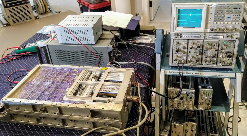
The photo below shows the physical implementation of the AGC's circuitry. This module implements four bits of the registers and arithmetic unit. The flat-pack ICs are the black rectangles; each module has two boards with 60 chips each, for a total of 240 NOR gates. The arithmetic unit and registers are built from four identical modules, each handling four bits; this is similar to a bit-slice processor.
Executing an instruction
This section illustrates the sequence of operations that the AGC performs to execute an instruction. In particular, I'll show how an addition instruction, ADS (add to storage), takes place. This instruction reads a value from memory, adds it to the accumulator (A register), and stores the sum in both the accumulator and memory. This is a single machine instruction, but the AGC performs many steps and many values move back and forth to accomplish it.
Instruction timing is driven by the core memory subsystem. In particular, reading a value from core memory erases the stored value, so a value must be written back after each read. Also, when accessing core memory there is a delay between when the address is set up and when the data is available. The result is that each memory cycle takes 12 time steps to perform first a read and then a write. Each time interval (T1 to T12) takes just under one microsecond, and the full memory cycle takes 11.7µs, called a Memory Cycle Time (MCT).
The MCT is the basic time unit for instruction execution. A typical instruction requires two memory cycles: one memory access to fetch the instruction from memory, and one memory access to perform the operation.13 Thus, a typical instruction requires two MCTs (23.4µs), yielding about 43,000 instructions per second. (This is extremely slow compared to modern processors performing billions of instructions per second.)
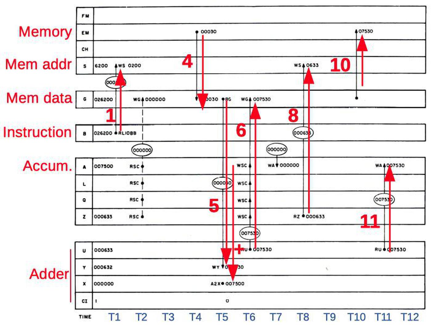
Internally, the Apollo Guidance Computer processes instructions by breaking an instruction into subinstructions, where each subinstruction takes one memory cycle For example, the ADS instruction consists of two subinstructions: the ADS0 subinstruction (which does the addition) and the STD2 subinstruction (which fetches the next instruction, and is common to most instructions). The diagram below shows the data movement inside the AGC to execute the ADS0 subinstruction. The 12 times steps are indicated left to right.
The important steps are:
T1: The operand address is copied from the instruction register (B) to the memory address register (S) to start a memory read.
T4: The operand is read from core memory to the memory data register (G).
T5: The operand is copied from (G) to the adder (Y).
The accumulator value (A) is copied to the adder (X).
T6: The adder computes the sum (U), which is copied to the memory data register (G).
T8: The program counter (Z) is copied to the memory address register (S) to prepare for fetching the next instruction from core memory.
T10: The sum in the memory data register (G) is written back to core memory.
T11: The sum (U) is copied to the accumulator (A).
Even though this is a simple add instruction, many values are moved around during the 12 time intervals. Each of these actions has a control signal associated with it; for instance, the signal A2X at time T5 causes the accumulator (A) value to be copied to the X register. Copying the G register to the Y register takes two control pulses: RG (read G) and WY (write Y). The next section will explain how the AGC's control unit generates the appropriate control signals for each instruction, focusing on these A2X, RG, and WY control pulses needed by ADS0 at time T5.
The control unit
As in most computers, the AGC's control unit decodes each instruction and generates the control signals that tell the rest of the processor (the datapath) what to do. The AGC is designed with microcoded approach, but the control signals are generated from a hardwired control unit built from NOR gates. Specifically, there are no microinstructions and the AGC does not have a control store holding microcode (which would have taken too much physical space).12You can think of the AGC as implementing the microcode ROM with highly-optimized logic gates.
The heart of the AGC's control unit is called the crosspoint generator. Conceptually, the crosspoint generator takes the subinstruction and the time step, and generates the control signals for that combination of subinstruction and time step. (You can think of the crosspoint generator as a grid with subinstructions in one direction and time steps in the other, with control signals assigned to each point where the lines cross.) For instance, going back to the ADS0 subinstruction, at time T5 the crosspoint generator would generate the A2X, RG, and WY control pulses, causing the desired data movement.
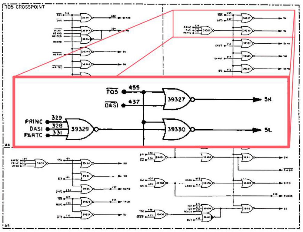
For efficiency, the implementation of the control unit is highly optimized. Instructions with similar behavior are combined and processed together by the crosspoint generator to reduce circuitry. For instance, the AGC has a "Double-precision Add to Storage" instruction (DAS). Since this is roughly similar to performing two single-word adds, the DAS1 subinstruction and ADS0 subinstruction share logic in the crosspoint generator. The schematic below shows the crosspoint generator circuitry for time T5, highlighting the logic for subinstruction ADS0 (using the DAS1 signal). For instance, the 5K signal is generated from the combination of DAS1 and T5.
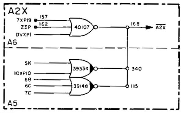
But what are the 5K and 5L signals? These are another optimization. Many control pulses often occur together, so instead of generating all the control pulses directly, the crosspoint generates intermediate crosspoint signals. For instance, 5K generates both the A2X and RG control pulses, while 5L generates the WY control pulse. The diagram below shows how the A2X signal is generated: any of 8 different signals (including 5K) generate A2X.15 Similar circuits generate the other control pulses. These optimizations reduced the size of the crosspoint generator, but it was still large, split across three modules in the AGC.
To summarize, the control unit is responsible for telling the rest of the CPU what to do in order to execute an instruction. Instructions are first decoded into subinstructions. The crosspoint generator creates the proper control pulses for each time interval and subinstruction, telling the AGC's registers, arithmetic unit, and memory what to do.14
Conclusion
This has been a whirlwind tour of the Apollo Guidance Computer's CPU. To keep it manageable, I've focused on the ADS addition instruction and a few of the control pulses (A2X, RG, and WY) that make it operate. Hopefully, this gives you an idea of how a computer can be built from components as primitive as NOR gates.
The most visible part of the architecture is the datapath: arithmetic unit, registers, and the data bus. The AGC's registers are built from simple NOR-gate latches. Even though the AGC's arithmetic unit can only do addition, the computer still manages to perform a full set of operations including multiplication and division and Boolean operations.9
However, the datapath is just part of the computer. The other critical component is the control unit, which tells the data path components what to do. The AGC uses an approach centered around a crosspoint generator, which uses highly-optimized hardwired logic to generate the right control pulses for a particular subinstruction and time interval.
Using these pieces, the Apollo Guidance Computer provided guidance, navigation, and control onboard the Apollo missions, making the Moon landings possible. The AGC also provided a huge boost to the early integrated circuit industry, using 60% of the United States' IC production in 1963. Thus, modern computers owe a lot to the AGC and its simple NOR gate components.
CuriousMarc has a series of AGC videos which you should watch for more information on the restoration project. I announce my latest blog posts on Twitter, so follow me @kenshirriff for future articles. I also have an RSS feed. Thanks to Mike Stewart for supplying images and extensive information.
Notes and references
-
The AGC restoration team consists of Mike Stewart (creator of FPGA AGC), Carl Claunch, Marc Verdiell (CuriousMarc on YouTube) and myself. The AGC that we're restoring belongs to a private owner who picked it up at a scrapyard in the 1970s after NASA scrapped it. ↩
-
In addition to the NOR-gate logic chips, the AGC used a second type of integrated circuit for its memory circuitry, a sense amplifier. (The earlier Block I Apollo Guidance Computer used NOR gate ICs that contained a single NOR gate.) ↩
-
How does the AGC stack up to early microprocessors? Architecturally, I'd say it was more advanced than early 8-bit processors like the 6502 (1975) or Z-80 (1976), since the AGC had 15 bits instead of 8, as well as more advanced instructions such as multiplication and division. But I consider the AGC less advanced than the 16-bit Intel 8086 (1978) which has a larger register set, advanced indexing, and instruction queue. Note, though, that the AGC was in a class of its own as far as I/O, with 227 interface circuits connected to the rest of the spacecraft.
Looking at transistor counts, the Apollo Guidance Computer had about 17,000 transistors in total in its ICs, which puts it between the Z80 microprocessor (8,500 transistors) and the Intel 8086 (29,000 transistors).
As far as performance, the AGC did a 15-bit add in 23.4μs and a multiply in 46.8μs. The 6502 took about 3.9μs for an 8-bit add (much faster, but a smaller word). Implementing an 8-bit multiply loop on the 6502 might take over 100μs, considerably worse than the AGC. The AGC's processor cycle speed of 1.024 MHz was almost exactly the same as the Apple II's 1.023 MHz clock, but the AGC took 24 cycles for a typical instruction, compared to 4 on the 6502. The big limitation on AGC performance was the 11.7μs memory cycle time, compared to 300 ns for the Apple II's 4116 DRAM chips. ↩
-
An AGC instruction fit into a 15-bit word and consisted of a 3-bit opcode and a 12-bit memory address. Unfortunately, both the opcode and memory address were too small, resulting in multiple workarounds that make the architecture kind of clunky.
The AGC's 15-bit instructions included a 12-bit memory address which could only address 4K words. This was inconvenient since the AGC had 2K words of core RAM and 36K words of core rope ROM. To access this memory with a 12-bit address, the AGC used a complex bank-switching scheme with multiple bank registers. In other words, you could only access RAM in 256-word chunks and ROM in somewhat larger chunks.
The AGC's instructions had a 3-bit opcode field, which was too small to directly specify the AGC's 34 instructions. The AGC used several tricks to specify more opcodes. First, an
EXTENDinstruction changed the meaning of the following instruction, allowing twice as many opcodes but wasting a word. Also, some AGC opcodes didn't make sense if performed on a ROM address (such as incrementing), so four different instructions ("quartercode instructions") could share an opcode field. Instructions that act on peripherals only use 9 address bits, freeing up 3 additional bits for opcode use. This allows, for instance, Boolean operations (AND, OR, XOR) to fit into the opcode space, but they can only access peripheral addresses, not main memory addresses.The AGC also used some techniques to keep the opcode count small. For example, it had some "magic" memory locations such as the "shift right register". Writing to this address performed a shift; this avoided a separate opcode for "shift right".
The AGC also had some instructions that wedged multiple functions into a single instruction. For instance, the "Transfer to Storage" instruction not only transferred a value to storage, but also checked the overflow flag and updated the accumulator and skipped an instruction if there had been an arithmetic overflow. Another complex instruction was "Count, Compare, and Skip", which loaded a value from memory, decremented it, and did a four-way branch depending on its value. See AGC instruction set for details. ↩
-
For more on the AGC's architecture, see the Virtual AGC and the Ultimate Apollo Guidance Computer Talk. ↩
-
The NAND gate also has the same property of being a universal gate. (In modern circuits, NAND gates are usually more popular than NOR gates for technical reasons.) The popular NAND to Tetris course describes how to build up a computer from NAND gates, ending with an implementation of Tetris. This approach starts by building a set of logic gates (NOT, AND, OR, XOR, multiplexer, demultiplexer) from NAND gates. Then larger building blocks (flip flop, adder, incrementer, ALU, register) are built from these gates, and finally a computer is built from these building blocks. ↩
-
Modern computers usually have a stack that is used for subroutine calling and returning. However, the AGC (like many other computers of its era) didn't have a stack, but stored the return address in a link register (the AGC's Q register). To use recursion, a programmer would need to implement their own stack. ↩
-
A carry-skip circuit improves the performance of the adder. The problem with binary addition is that propagating a carry through all the bits is slow. For example, if you add 111111111111111 + 1, the carry from the low-order bit gets added to the next bit. This generates a carry which propagates to the next bit, and so forth. This "ripple carry" causes the addition to be essentially one bit at a time. To avoid this problem, the AGC uses a carry-skip circuit that looks at groups of four bits. If there is a carry in, and each position has at least one bit set, there is certain to be a carry, so a carry-out is generated immediately. Thus, propagating a carry is approximately three times as fast. (With groups of four bits, you'd expect four times as fast, but the carry-skip circuit has its own overhead.) ↩
-
You might wonder how the AGC performs a variety of arithmetic and logic operations if the arithmetic unit only supports addition. Subtraction is performed by complementing one value (i.e. flipping the bits) and then adding. Most computers have a complement circuit built into the ALU, but the AGC is different: when the B register is read, it can provide either the value or the complement of the stored value.10 So to subtract a value, the value is stored in the B register and then the complement is read out and added.
What about Boolean functions? While most computers implement Boolean functions with logic circuitry in the ALU, the Apollo Guidance Computer manages to implement them without extra hardware. The OR operation is implemented through a trick of the register circuitry. By gating two registers onto the write bus at the same time, a 1 from either register will set the bus high, yielding the OR of the two values. AND is performed using the formula A ∧ H = ~(~A ∨ ~H); complementing both arguments, doing an OR, and then complementing the result yields the AND operation. XOR is computed using the formula A ⊕ H = ~(A ∨ ~H) ∨ ~(H ∨ ~A), which uses only complements and ORs. It may seem inefficient to perform so many complement and OR operations, but since the instruction has to take 12 time intervals in any case (due to memory timing), the multiple steps don't slow down the instruction.
Multiplication is performed by repeated additions, subtractions, and shifts using a Radix-4 Booth algorithm that operates two bits at a time. Division is performed by repeated subtractions and shifts.11 Since multiply and divide require multiple steps internally, they are slower than other arithmetic instructions. ↩
-
Since a latch has outputs for both a bit and the complement of the bit, it is straightforward to get the complemented value out of a latch. Look near the bottom of the schematic to see the B register's circuitry that provides the complemented value. ↩
-
The AGC's division algorithm is a bit unusual. Instead of subtracting the divisor at each step, a negative dividend / remainder is used through the division and the divisor is added. (This is essentially the same as subtracting the divisor, except everything is complemented.) See Block II Machine Instructions section 32-158 for details. ↩
-
The AGC doesn't use microcode but confusingly some sources say it was microprogrammed. The book "Journey to the Moon" by Eldon Hall (creator of the AGC) says:
The instruction selection logic and control matrix was a microprogrammed instruction sequence generator, equivalent to a read-only memory implemented in logic. Outputs of the microprogrammed memory were a sequence of control pulses that were logic products of timing pulses, tests of priority activity, instruction code, and memory address.
This doesn't make sense, since the whole point of microprogramming is to use read-only memory instead of hardwired control logic. (See A brief history of microprogramming, Computer architecture: A quantitative approach section 5.4, or Microprogramming: principles and practices.) Perhaps Hall means that the AGC's control was "inspired" by microprogramming, using a clearly-stated set of sequenced control signals with control hardware separated from the data path (like most modern computers, hardwired or microcoded). (In contrast, in many 1950s computers (like the IBM 1401) each instruction's circuitry generated its own ad hoc control signals.)
By the way, implementing the AGC in microcode would have required about 8 kilobytes of microcode (79 control pulses for about 70 subinstructions with 12 time periods. This would have been impractical for the AGC, especially when you consider that microcode storage needs to be faster than regular storage. ↩
-
While instructions typically used two subinstructions, there were exceptions. Some instructions, such as multiply and divide, required multiple subinstructions because they took many steps. On the other hand, the jump instruction (TC) used a single subinstruction since fetching the next instruction was the only task to do. ↩
-
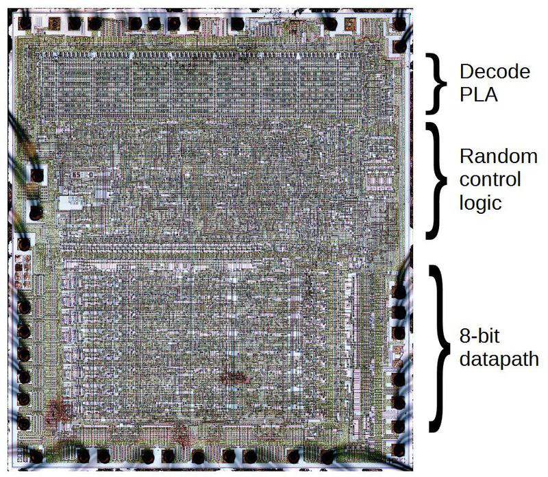
Other processors use different approaches to generate control signals. The 6502 and many other early microprocessors decoded instructions with a Programmable Logic Array (PLA), a ROM-like way of implementing AND-OR logic. The Z-80 used a PLA, followed by logic very similar to the crosspoint generator to generate the right signals for each time step. Many computers use microcode, storing the sequence of control steps explicitly in ROM. Since minimizing the number of chips in the AGC was critical, optimizing the circuitry was more important than using a clean, structured approach.
Die photo of the 6502 microprocessor. The 6502 used a PLA and random logic for the control logic, which occupies over half the chip. Note the regular, grid-like structure of the PLA. Die photo courtesy of Visual 6502. -
Each subinstruction's actions at each time interval are described in the manual. The control pulses are described in detail in the manual. (The full set of control pulses for ADS0 are listed here.) ↩



11 comments:
Thanks! I've been waiting for this one!
Thinking of the core rope memory, from your description a 'value of '1' requires looping through a core, while a '0' bypasses a core. It seems like therefore a '1' weighs more than a zero, in terms of flying weight of the core rope module. If that is true, I wonder how much more a '1' in core rope weighs? I read here that a single core can be used for multiple bits, so the extra weight of a core is shared by the number of wires running through it representing a '1' bit. I'm sure that statistically the overall percentages of '1's and '0's is close to 50/50 looking at instruction encoding and the SW in ROM. If there were a large difference it could imply an inefficiency. For example if the instruction encoding was such that many instructions were mostly '0's, perhaps the instruction word should use less bits. Knowing there may have been a few versions of the rope core, as the SW matured, I wonder if the weight of the versions differed due to the number of cores required to implement the binary image in each version? PS - thanks for these interesting posts about the AGC. What a unique and significant piece of computing hardware!
An excellent read is "The Apollo Guidance Computer: Architecture and Operation," Frank O'Brien, 2010, Praxis Publishing, Ltd.
My brother, Dale Randolph, worked for North American Rockwell in the late 1960s. He spent about three years on the software for the Saturn Rocket (Apollo) computers including a year in Cape Canaveral leading up to the first Apollo launch.
Thank you for the details of this computer, a unique system.
Someone has compared the AGC's computational power against that of a USB charger:
https://forrestheller.com/Apollo-11-Computer-vs-USB-C-chargers.html
I've watched the entire series of Marc's with the team that rebuilt the AGC, great stuff!
That said, I'm confused by comments that this AGC enthusiast mentions about a code "interpreter" for the AGC: https://youtu.be/B1J2RMorJXM?t=2214
If there was an interpreter and logically, a compiler, you wouldn't have fully-commented assembly language, as exists in Marc's many pages of print-outs.
Was this "interpreter" this person is talking about some kind of simulation, run on mainframes?
Also, it's probably semantics, but the mention of an "operating system" is a little odd, since I would expect that the AGC would run code in a linear fashion until externally interrupted, as far as I understand, there's no overarching "OS" controlling execution of subprograms.
I'm also a little fuzzy on the concept that the AGC could "do many things at once", but so can a generic microcontroller running a large program loop; you get the impression of many things being done "at once", but its really just sequential, albeit done very quickly. (I've designed simple GPS telemetry recording systems with display, recording to SD, etc.)
Your thoughts would be greatly appreciated!
I am fairly familiar with the PDP8 style computers and know that the core logic it used required a read/write cycle to retain memory. That is when you read magnetic core memory you lost the value and it had to be rewritten. Was it similar in the AGC?
Where can I get a dual 3-input NOR gate chip used in the AGC? I would like to re build it.
@AGCBubba: No, the computer could indeed be programmed both directly in assembler and in this other, interpreted, high(er)-level language. Assembly code would run directly on the AGC's CPU, whereas for the interpreter language, the AGC's ROM contained a program implementing a virtual machine which could be invoked and would then execute code written in that interpreted language.
Both kinds of code can be intermixed in the assembly listings and the assembler took care of transforming each kind of statement to the correct machine code.
Some more (and perhaps better) explanations can be found here:
https://www.ibiblio.org/apollo/assembly_language_manual.html#The_Interpreter_vs._the_CPU
https://www.ibiblio.org/apollo/assembly_language_manual.html#MarkSchulman
As for the bits about "operating system" and "do many things at once": The software for the AGC did actually support preemptive multitasking of various subprograms, so the OS moniker for the code controlling that doesn't seem that inappropriate.
Don Eyle's page has some description on how this worked:
https://www.doneyles.com/LM/Tales.html
Thanks for documenting all this amazing stuff! I laid out a recreation of above register-adder circuit using five SN74HCS27DR (CMOS triple 3-input NOR) gates in SOIC-14 packs. Along with the fifteen header pins, the module is 2"x0.6".
Thanks for documenting all this amazing stuff! I recreated the above register-adder using five SN74HCS27DR (CMOS Triple 3-input NOR) in SOIC14 packs. With 15 header pins, the module is 2 x 0.6 inches.
Post a Comment