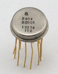
I recently obtained a mysterious electronic component in a metal can, flatter and slightly larger than a typical integrated circuit.1 After opening it up and reverse engineering the circuit, I determined that this was an op amp built for NASA in the 1960s using hybrid technology. It turns out that the development of this component ties connected several important people in the history of semiconductors, and one of these op amps is on the Moon.
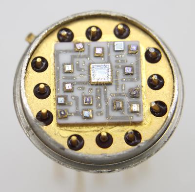
To determine what this component did and how it worked, I sawed the top off the metal can with a jeweler's saw, revealing the circuitry inside. There wasn't an integrated circuit inside but a larger hybrid module, built from tiny individual transistors on a ceramic substrate. In the photo below, the ceramic wafer has grayish conductive traces printed on it, similar to a printed circuit board. Individual silicon transistors (the smaller shiny squares) are attached to the traces on the ceramic. Thin gold wires connect the components together, and connect the circuit to the external pins.
Hybrid circuitry was widely used in the 1960s before complex circuits could be put on an integrated circuit. (The popular IBM System/360 computers (1964), for instance, were built from hybrid modules rather than ICs.) Although integrated circuit op amps were first produced in 1963, hybrids could avoid limitations of IC manufacturing and produce better performance, so hybrids remained popular in the 1970s and even 1980s.
At first, I couldn't identify this part, so I asked op amp expert Walt Jung for help. He identified the "a" on the package for Amelco, which helped me track down the rather obscure 2404BG op amp manufactured by the now-forgotten company Amelco.2 This part sold in 1969 for $58.50 each (equivalent to about $300 today). In comparison, you can get a modern JFET quad op amp for under 25 cents.
Some op amp history
The op amp is one of the most popular components of analog circuits because of its flexibility and versatility. An op amp takes two input voltages, subtracts them, multiplies the difference by a huge value (100,000 or more), and outputs the result as a voltage. In practice, a feedback circuit forces the inputs to be nearly equal; with an appropriate feedback circuit, an op amp can be used as an amplifier, a filter, integrator, differentiator, or buffer, for instance. A key figure in the early development of op amps was George Philbrick who started a company of the same name. The commercial history of the op amp started in 1952 when Philbrick introduced the K2-W op amp, a two-tube module that made op amps popular.3
I'll now jump to Jean Hoerni, who founded Amelco. One of the key events in the history of Silicon Valley was the 1957 departure from Shockley Semiconductor of eight employees, known as the "traitorous eight". They founded Fairchild, which led to dozens of startups and the growth of Silicon Valley. (Moore and Noyce, two of the eight, later left Fairchild to found Intel.) Physicist Jean Hoerni, of the traitorous eight, worked at Fairchild to improve transistors and succeeded beyond anyone's expectations. In 1959, he invented the planar transistor in 1959, which revolutionized semiconductor fabrication. (The planar process is essentially the technique used in modern transistors and ICs, using masks and diffusion on a flat silicon die.) Interestingly, the transistors in the op amp module (below) look identical to Hoerni's original teardrop-shaped planar transistors. Transistors from the 1970s and later look entirely different, so it was a bit surprising to find Hoerni's original design in use in this module.
Hoerni left Fairchild in 1961 and helped found a company called Amelco. It focused on semiconductors for space applications, avoiding direct competition with Fairchild. Linear (analog) integrated circuits were a major product for Amelco, with Amelco building op amps for Philbrick (the pioneering op amp company). Amelco also manufactured discrete transistors using Hoerni's planar process. At Amelco, Hoerni developed a technique to built a type of transistor called a JFET using his planar process, and these transistors became one of Amelco's most popular products. The key benefit of a JFET is that the input current to the transistor's gate is extraordinarily small, an advantage for applications such as op amps. Amelco used Hoerni's JFET in the industry's first JFET op amp, producing a high-performance op amp.
Bob Pease,4 a famous analog circuit designer, ties these threads together. In the 1960s, Bob Pease designed op amps for Philbrick, including the Q25AH hybrid FET op amp (1965). Amelco manufactured this op amp for Philbrick, so Bob Pease visited Amelco to help them with some problems. The story (here and here) is that during his visit Bob Pease got in a discussion with some Amelco engineers about NASA's requirements for a new low-power, low-noise amplifier. Bob Pease proceeded to design an op amp during his coffee break that met NASA's stringent requirements. This op amp was used in a seismic probe that Apollo 12 left on the Moon in 1969, so there's one of these op amps on the Moon now. Amelco marketed this op amp as the 2401BG.
As for the 2404BG I disassembled, its circuitry is very similar to Bob Pease's 2401BG design5, so I suspect he designed both parts. The 2404BG op amp also made it to the Moon; it was used in the high voltage power supply of the Lunar Atmosphere Composition Experiment (LACE). LACE was a mass spectrometer left on the Moon by the Apollo 17 mission in 1972. (LACE determined that even though the moon has almost no atmosphere, it does has some helium, argon, and possibly neon, ammonia, methane and carbon dioxide.)
In 1966 Amelco merged with Philbrick, forming Teledyne Philbrick Nexus which after some twists and turns was eventually acquired by Microchip Technology in 2000. (Among other things, Microchip produces the AVR microcontrollers used in the Arduino.)
Inside the hybrid op amp
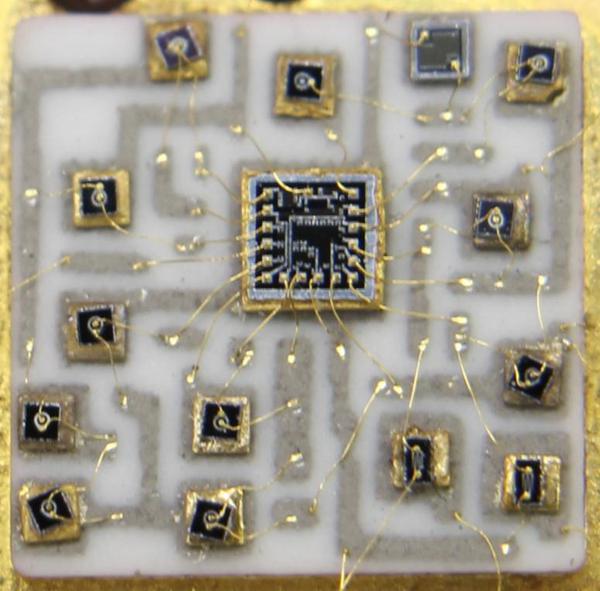
In this section, I'll describe the construction and circuitry of the 2404BG op amp in more detail. The photo below shows a closeup of the ceramic wafer and the components on it. The grayish lines on the ceramic are conductive circuit traces. Most of the squares are NPN and PNP transistors, each on a separate silicon die. The underside of the die is the transistor's collector, connected to a trace on the ceramic. Tiny gold wires are attached to the emitter and base of the transistor, wiring it into the circuit. The two rectangular transistors in the lower right are the JFETs. The large square in the middle is a collection of resistors, and a single resistor is in the upper right. Note that unlike integrated circuits that can be mass-produced on a wafer, hybrid modules required a large amount of expensive mechanical processing and wiring to mount and connect the individual components.
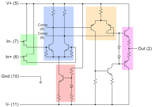
I reverse engineered the circuitry of the op amp module and generated the schematic below.6 This circuit is fairly simple as op amps go, with about half the components of the classic 741 op amp. The inputs are buffered by the JFETs (green). The differential pair (blue), amplifies the input, directing current down one side of the pair or the other. The current source (red) generates a tiny fixed current for the differential pair using a current mirror circuit. The second stage amplifier (orange) provides additional amplification. The output transistors (purple) are set up in a class AB configuration to drive the output. The remaining components (uncolored) bias the output transistors. External capacitors on the compensation pins (8 and 9) prevent the op amp from oscillating.
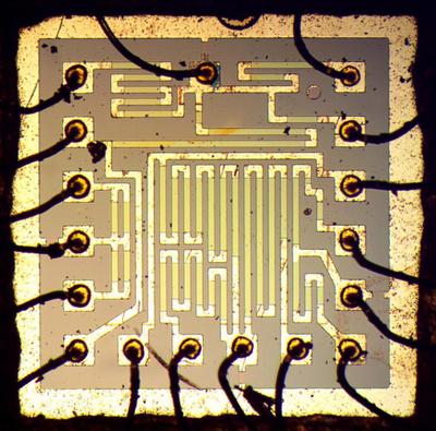
Most of the resistors are on the single die in the middle of the module; this die is 1.7mm (1/16") on a side. The zig-zag shapes are thin-film resistors constructed from tantalum deposited on an oxide-coated silicon wafer. (One advantage of hybrid circuitry over integrated circuits was more accurate and better quality resistors.) The resistance is proportional to the length, so the meandering shapes allowed larger resistors to fit on the die. Around the outside of the die are metal pads; the bond wires attached to the pads connected the resistors to other parts of the circuit. Note the small circle to the left of the upper right pad; one innovation at Amelco was "mark-in-mark" targets to align the masks used for different layers of a chip.
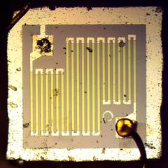
The current source circuit needed a very high-valued resistor, so it used a separate resistor die (below). This resistor used a long, thinner trace to produce a higher resistance than the resistors on the previous die. Note the circular alignment target in the lower right. The die for this resistor is 0.8mm on a side.
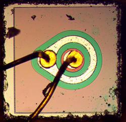
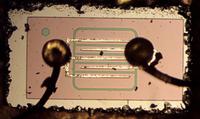
The photo below shows one of the junction FET transistors used in the op amp. The metal fingers connect to source and drain regions. The gate (green) is connected underneath. This design is almost identical to the first planar JFET that Hoerni invented in 1963. It was initially difficult to produce high-quality JFETs on an integrated circuit, which motivated the production of hybrid JFET op amps. It wasn't until 1974 that National Semiconductor engineers developed the ion implantation technique for fabricating consistent, high-quality JFETs and used this "BIFET" technique to build better JFET op amp integrated circuits.
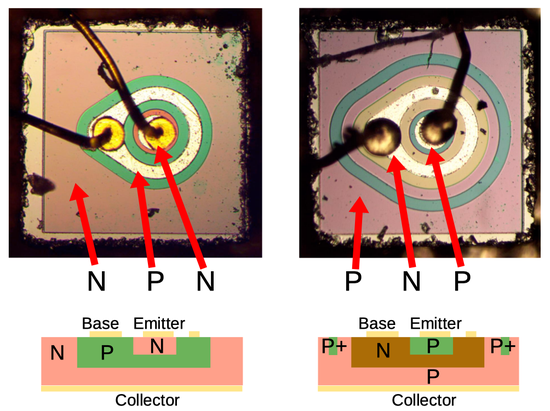
The diagram below compares the structure of the NPN and PNP transistors in the module, with photos at top and a cross-section diagram below.
Each transistor starts with a square die of silicon, which is doped with impurities to form N and P regions with different properties. The N and P doped silicon show up as different colors under the microscope. The shiny metal layer on top is visible, with one bond wire attached to the central emitter. A second bond wire is attached to the base region surrounding the emitter; the "teardrop" shape provides a wider area to attach the base wire. The underside of the die is the collector, which makes contact with the wiring on the ceramic wafer. The NPN transistor follows the straightforward planar structure. The PNP transistor, however, required an extra "annular ring" to operate at the op amp's higher voltages.7
Conclusions
This random component that I opened up turned out to have a more interesting history than I expected. It ties together the early days of op amps with Philbrick, Bob Pease's analog circuit development, now-forgotten Amelco, and NASA's scientific experiments on the Moon. The transistors inside this module were built using Hoerni's original planar designs, providing a glimpse into the development of the planar process that revolutionized semiconductors. Finally, this op amp shows the capabilities of hybrid technology, now almost completely eliminated by integrated circuits.
If you enjoyed this look inside a hybrid op amp, you may also like my analysis of another JFET op amp and the famous 741 op amp. I announce my latest blog posts on Twitter, so follow me at @kenshirriff. I also have an RSS feed. Thanks to op amp guru Walt Jung for help identifying the module.
Notes and references
-
The module was packaged in a standard 12-pin TO-8 package. Most metal can integrated circuits are in the smaller TO-5 package, but the larger hybrid circuits require more room. ↩
-
The "15818" on the package is a CAGE code, a NATO identifier used to track suppliers. Originally, 15818 was assigned to Amelco; due to mergers, this number now shows up as TelCom Semiconductor. ↩
-
Several sources provided much of the information for this blog post. The book History of Semiconductor Engineering discusses in great detail the history of various semiconductor companies and the people involved. For an extremely detailed history of op amps, including the development of JFET op amps in the 1970s, see Op Amp History by Walt Jung, along with his Op Amp Applications Handbook. IC Op-Amps Through the Ages also has a history of op amps. ↩
-
Bob Pease wrote a popular column "Pease Porridge" on analog circuits. He also wrote books such as Troubleshooting Analog Circuits. ↩
-
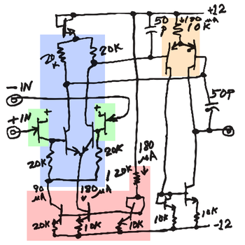
Bob Pease's article What’s All This 2401BG Stuff, Anyhow? (page 54) provides a schematic of the 2401BG (below). Comparing the schematics, the 2401BG is very similar to the 2404BG that I examined. (I've colored the functional blocks to match my 2404BG schematic to make comparison easier.)
Bob Pease's schematic of the 2401BG hybrid op amp that he designed for NASA.The main difference is the output stage: the 2401BG takes the output directly from the second amplifying pair (with a current mirror at the bottom to sink current), while the 2404BG adds a class AB output stage. The 2401BG also has a separate current mirror for the bases of the input NPN transistors. ↩
-
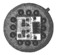
After I reverse-engineered the op amp schematic, I found a 1968 databook with a schematic for an Amelco hybrid op amp. The two schematics are almost identical, except the databook schematic includes two compensation capacitors, which are external on the 2404BG.
Photo of an Amelco hybrid op amp.The databook provided the above photo of the hybrid op amp, which is completely different from the 2404BG I examined. The databook did not give a part number (which is unusual for a databook), so I suspect this was a version of the 2404BG under development at the time. ↩
-
You'd expect NPN and PNP transistors to be symmetrical, but the PNP transistors needed to be different to support high-voltage operation. The problem was that an interaction between the P region and the silicon dioxide on top caused N-type properties in a thin layer of the weakly-doped P region. At higher voltages, this could cause the transistor to short out. The solution was to create a strongly-doped P+ "annular ring" to interrupt this unwanted N behavior. Details in Jack Haenichen oral history and patent 3226611. ↩
16 comments:
Very interesting to learn about the history.
Is there anything left to invent for the average engineer?
It appears to be an annular ring.
See:
http://www.semiconductormuseum.com/Transistors/Motorola/Haenichen/Haenichen_Page7.htm
and the next page too.
Thank you William for the link. I've updated the post with information about the annular ring.
Ken I counted 11 transistors in the die picture, but schematics shows only 10. Is it correct?
Andrei: The die has 13 transistors (11 bipolar, 2 JFET), but three are wired as diodes, so I drew them as diodes on the schematic.
Hi Ken, another great blog post. Thanks!
You might be interested to know Paul Carlson featured and operated a K2-W on his YouTube channel: https://www.youtube.com/watch?v=mEFdADrU9MA
Amazing !
as in the 60's they manage to perform welding wires of components so small, would it be manual?
@Richard: They had lots of magnifying devices in that time, like the ones on pages 13 and 54 of this tube propaganda booklet: http://www.rcaselectron.com/TubesAndTransistors.pdf Though they seem to be of the shadow projection (light from below) type not the metallurgical (reflective) type.
Richard, to attach the wires they'd use a wire bonding machine, same as for producing integrated circuits or transistors. It would have a stereo microscope and a manual positioning mechanism, so the operator would move to the right spot and then move a lever to attach the wire. Diagrams of a wire bonding machine are here. From what I read, automatic wire bonding machines became popular in the 1980s.
Awesome Ken, I always learn something new from your posts. I look forward to your next one!
Ken THANKS so much for this! I thought I was way cool in 1968 when I used the new Philbrick Plastic Case-Edge connector opamps to build a automatic logging system for Broadcast Transmitters. The Philbrick book was my bible. Two of my sons who saw that development work in our basement are Engineers and Chip Designers today, and two Grandsons are Engineers. At 79 I still love designing circuits and writing code to help younger people learn and love electronics. Now I'm aiming at Elementary/Middle School with this:
https://arduinoinfo.mywikis.net/wiki/EasyConnectKit
In awe of what you do, and in fond memory of Bob Pease,
Regards, Terry King
...In The Woods in Vermont, USA
[email protected]
Nice writeup as always, but one typo correction. In the "inside the hybrid op amp section" you have "Tiny gold wires are attached to the emitter and collector of the transistor..." Should have been base instead of collector. I suspect anyone reading this knew what you meant but figured I'd mention it.
Thanks Ken Shirriff for the clarifications.
Thank you Zom-B, great stuff.
I imagine the probability of manufacturing error to be manual should be high.
Bell Labs came up with wire bonding in the mid-50s: https://nepp.nasa.gov/index.cfm/20911
One of my colleagues designed a hybrid in the late 80s with about 200 dice. He and another colleague manually wirebonded the first two prototypes. I seem to recall there were over 2000 wires on the completed assembly. Most of the chips were commodity parts but the manufacturers hadn't released them in an SMD package yet. By the time they did, we had an ASIC designed and fabbed to do the same thing.
I designed a couple of hybrids using custom ASICs myself, fortunately they were regular enough to allow for automated wirebonding. When the first article of one came back from fabrication, our assembler accidently brushed it and caused some short circuits so I had to mount it on a stage under a microscope and carefully tease a few loops apart. It took a few passes to not introduce more shorts as I cleared them out. If memory serves, they were on a 10 mil pitch in two layers or levels.
Unless I'm mistaken Microchip makes the PIC micro-controllers. The AVRs used in the Arduinos come from Atmel.
Microchip acquired Atmel over three years ago, so PICs and AVRs are now Microchip products.
Post a Comment