The structure of the integrated circuit
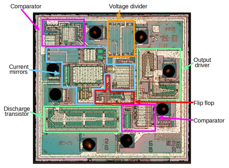
The photo below shows the silicon die of the LMC555 as seen through a microscope, with the main function blocks labeled (photo from Zeptobars). The die is very small, just over 1mm square. The large black circles are connections between the chip and its external pins. A thin layer of metal connects different parts of the chip. This metal is clearly visible in the photo as white lines and regions. The different types of silicon on the chip appear as different colors. Regions of the chip are treated (doped) with impurities to change the electrical properties of the silicon. N-type silicon has an excess of electrons (making it Negative), while P-type silicon lacks electrons (making it Positive). On top of the silicon, polysilicon wiring shows up as other colors. The silicon regions and polysilicon are the building blocks of the chip, forming transistors and resistors, which are connected by the metal layer.
A brief explanation of the 555 timer
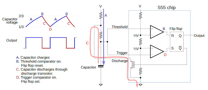
The 555 chip is extremely versatile with hundreds of applications from a timer or latch to a voltage-controlled oscillator or modulator. To explain the chip, I will use one of the simplest circuits, an oscillator that cycles on and off at a fixed frequency.The diagram below illustrates the internal operation of the 555 timer used as an oscillator. An external capacitor is repeatedly charged and discharged to produce the oscillation. Inside the 555 chip, three resistors form a divider generating reference voltages of 1/3 and 2/3 of the supply voltage. The external capacitor will charge and discharge between these limits, producing an oscillation, as shown on the left. In more detail, the capacitor will slowly charge (A) through the external resistors until its voltage hits the 2/3 reference. At that point (B), the threshold (upper) comparator switches the flip flop off turning the output off. This turns on the discharge transistor, slowly discharging the capacitor (C) through the resistor. When the voltage on the capacitor hits the 1/3 reference (D), the trigger (lower) comparator turns on, setting the flip flop and the output on, and the cycle repeats. The values of the resistors and capacitor control the timing, from microseconds to hours.
To summarize, the key components inside the 555 timer are the comparators to detect the upper and lower voltage limits, the three-resistor divider to set these limits, the flip flop to keep track of whether the circuit is charging or discharging, and the discharge transistor. The 555 timer has two other pins (reset and control voltage) that I haven't covered above; they are used in more complex circuits.
Transistors inside the IC
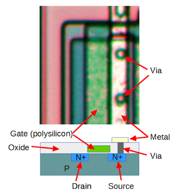
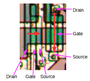
Like most integrated circuits, the CMOS 555 timer chip is built from two types of transistors, PMOS and NMOS. In contrast, the classic 555 timer uses the older technology of bipolar transistors (NPN and PNP). CMOS is popular because it uses much less power than bipolar. CMOS transistors be packed into a chip very densely without overheating, which is why CMOS has ruled the microprocessor market since the 1980s. Although the 555 doesn't require many transistors, low power consumption is still an advantage.The diagram below shows an NMOS transistor in the chip, with a cross section below. Since the transistor is built from overlapping layers, the die photo is a bit tricky to understand, but the cross section should help clarify it. The different colors in the silicon indicate regions that has been doped to form N and P regions. The green rectangle is polysilicon, a layer above the silicon. The whitish rectangle is the metal layer on top. The vias are connections between the layers.
A MOS transistor can be thought of as a switch that connects or disconnects the source and drain, based on the voltage on the gate. The transistor consists of two rectangular strips of silicon that has been doped negative (N), embedded in the underlying P silicon. The gate consists of a layer of conductive polysilicon above and between the drain and source. The gate is separated from the underlying silicon by a very thin layer of insulating oxide. If voltage is applied to the gate, it produces an electric field that changes the properties of the silicon below the gate, allowing current to flow.[2] The photo also shows the metal connection to the source, along with the "vias" that connect the silicon layer to the metal layer through the insulating oxide.[3]
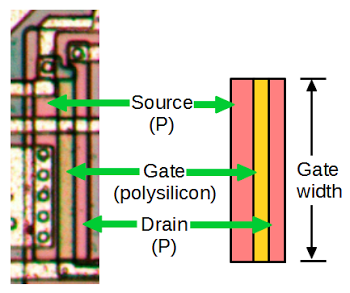
The second type of transistor is PMOS, shown below. PMOS transistors are opposite to NMOS in many ways; they are called complementary, which is the C in CMOS. PMOS uses a source and drain of P-doped silicon embedded in N-doped silicon. The transistor is turned on by a low voltage on the gate (opposite to NMOS), causing current to flow from the source to drain. The metal connections to the source, gate, and drain are visible below, with circular vias to the underlying layers. (Note that the diagram on the right is not a cross section, but a simplified "overhead" view.) In the die photo, NMOS transistors are blue with a green gate, while PMOS transistors are pink with orange gates. These colors are created by interference due to the thickness of the layers, and saturation is enhanced in the photo.
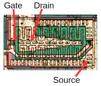
The output transistors in the 555 are much larger than the other transistors and have a different structure in order to produce the high-current output. The photo below shows one of the output transistors. Note the zig-zag structure of the gate, between the source (outside) and drain (center). Also note that the metal layer for the drain is narrow on the right and widens as it exits the transistor in order to handle the increasing current.[4]
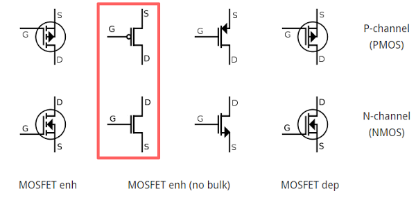
A variety of symbols are used to represent MOS transistors in schematics; the diagram below shows some of them. In this article, I use the highlighted symbols.
How resistors are implemented in silicon
Resistors are a key component of analog circuits. Unfortunately, resistors in ICs are large and inaccurate; the resistances can vary by 50% from chip to chip. Thus, analog ICs are designed so only the ratio of resistors matters, not the absolute values, since the ratios remain nearly constant even if the values vary depending on manufacturing conditions.
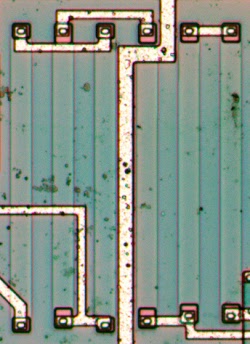
The photo above shows the resistors that form the voltage divider in the chip. There are six 50kΩ resistors, connected in series to form three 100kΩ resistors. The resistors are the pale vertical rectangles. At the end of each resistor, a via and P+ silicon well (pink square) connects the resistor to the metal layer, which wires them together. The resistors themselves are probably P-doped silicon.
To reduce current, the CMOS chip uses 100kΩ resistors, much larger than the 5kΩ resistors in the bipolar 555 timer. Urban legend says that the 555 is named after these three 5K resistors, but according to its designer 555 is just an arbitrary number in the 500 chip series
IC component: The current mirror
There are some subcircuits that are very common in analog ICs, but may seem mysterious at first. The current mirror is one of these. If you've looked at analog IC block diagrams, you may have seen the symbols below, indicating a current source, and wondered what a current source is and why you'd use one.
The idea of the current mirror is you start with one known current and then you can "clone" multiple copies of the current with a simple transistor circuit, the current mirror. A common use of a current mirror is to replace resistors. As explained earlier, resistors inside ICs are both inconveniently large and inaccurate. It saves space to use a current mirror instead of a resistor whenever possible. Also, the currents produced by a current mirror are nearly identical, unlike the currents produced by two resistors.
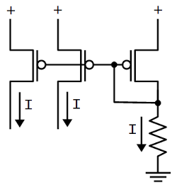
The circuit below shows how a current mirror is implemented with three identical transistors.[5] A reference current passes through the transistor on the right. (In this case, the current is set by the resistor.) Since all the transistors have the same emitter voltage and base voltage, they source the same current, so the currents on the left match the reference current on the right. For more flexibility, you can modify the relative sizes of the transistors in the current mirror and make the copied current larger or smaller than the reference current.[4] The CMOS 555 chip uses a variety of transistor sizes to control the currents in the circuit.
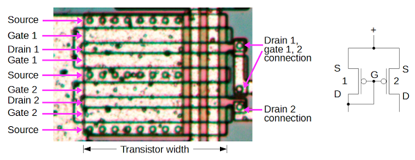
The diagram below shows one of the current mirrors in the LMC555 chip, formed from two transistors. Each transistor is actually two transistors in parallel, which is a common trick in the chip, so there are physically two pairs of transistors. It's a bit tricky to see the transistors because the metal layer partially covers them, but hopefully the description will make sense. Starting at the top, the first transistor is formed from the wide rectangles for source, gate 1, and drain 1. Note the vias connecting the metal layer to the source. The next transistor shares drain 1, with the second gate 1 and source below. Since these two transistors share the drain, and the sources and gates are wired the same, the two transistors effectively form one larger transistor. Likewise, there are two transistors below in parallel: source, gate 2, drain 2, and then drain2, gate2, source.
The schematic on the right shows how the transistors are wired together as a current mirror. If you look at the photo carefully, you can see that a single polysilicon strip snakes back and forth to form all the gates, so the gates are connected together. On the right, the upper metal strip connects drain 1 and the gates to the rest of the circuit. The lower metal strip is connected to drain 2.
IC component: The differential pair
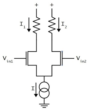
The second important circuit to understand is the differential pair, the most common two-transistor subcircuit used in analog ICs.[6] You may have wondered how a comparator compares two voltages, or an op amp subtracts two voltages. This is the job of the differential pair.
The schematic above shows a simple differential pair. The current source at the bottom sinks a fixed current I, which is split between the two input transistors. If the input voltages are equal, the current will be split equally into the two branches (I1 and I2). If one of the input voltages is a bit higher than the other, the corresponding transistor will conduct more current, so one branch gets more current and the other branch gets less. A small input difference is enough to direct most of the current into the "winning" branch, flipping the comparator on or off. Rather than resistors, the chip uses a current mirror on the two branches. This acts as an active load and increases the amplification.
Inverters and the flip flop
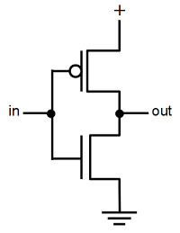
Although the 555 is an analog circuit, it contains a digital flip flop to remember its state. The flip flop is built out of inverters, simple logic circuits that turn a 1 into a 0 and vice versa. The 555 uses standard CMOS inverters, as shown below.
The inverter is built from two transistors. If the input is 0 (i.e. low), the PMOS transistor on top turns on, connecting the positive supply to the output, producing a 1. If the input is 1 (high), the NMOS transistor on the bottom turns on, connecting ground to the output, producing a 0. The magical part of CMOS is that the circuit uses almost no power. Current doesn't flow through the gate (because of the insulating oxide layer), so the only power usage is a tiny pulse when the output changes state, to charge or discharge the wire's capacitance.[7]
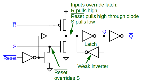
The diagram below shows the circuit for the flip flop. Two inverters are connected in a loop to form a latch. If the top inverter outputs 1, the bottom outputs 0, forming a stable cycle. If the top inverter outputs 0, the bottom outputs 1, again forming a stable cycle.
To change the value stored in the flip flop, the new value is simply forced into the latch, overriding the existing value with brute force. To make this work, the bottom inverter is "weak", using low-current transistors. This allows the set or reset inputs to overpower the weak inverter and the latch will immediately flip into the proper state The R (reset) and S (set) inputs come from the comparators and pull the latch input high or low through the transistors. Reset comes from the input pin and pulls the latch input high through a diode; the Reset inverter's output current is controlled by a current mirror. Reset will pull S low, blocking the action of a contradictory S input.
The 555 schematic interactive explorer
The 555 die photo and schematic below are interactive. Click on a component in the die or schematic, and a brief explanation of the component will be displayed. (For a thorough discussion of how the 555 timer works, see 555 Principles of Operation.)For a quick overview, the large output transistors and discharge transistor are distinguishable by their zig-zag gate pattern. The current mirror transistors are generally large. The threshold comparator consists of Q1 through Q5. The trigger comparator consists of Q13 through Q18. Q19 through Q29 form the flip flop circuit. The voltage divider resistors are in the upper center of the chip.[8]
I created the above schematic by reverse-engineering the chip, so I don't guarantee full correctness. A PDF of my schematic is here and a differently-formatted version is here. The schematic of a different CMOS 555 is here, and it's interesting to compare the differences. While the comparators are the same, the current mirrors are built differently, and the flip flop circuit is very different.
CMOS 555 compared with traditional bipolar 555
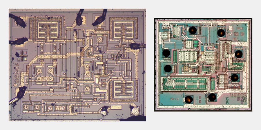
The regular 555 timer was designed in 1970, while a CMOS version (the ICM7555) wasn't released until 1978. The LMC555 described in this article came out around 1988, while the die itself has a date of 1996.The image below compares the classic 555 timer (left) with the CMOS LMC555 (right), both to the same scale. While the bipolar chip is constructed from silicon connected by a metal layer, the CMOS chip has an additional interconnect layer of polysilicon, which makes the chip more complex to understand visually. The CMOS chip is smaller. In addition, the CMOS chip has a lot of wasted space in the bottom and upper right, so it could have been made even smaller. The CMOS transistors are much more complex than the bipolar transistors. Except for the output transistors, the bipolar transistors are all simple individual units. Most of the CMOS transistors in comparison are built from two or more transistors in parallel. The classic 555 uses many more resistors than the CMOS 555; 16 versus 4.
You can see from the photo that the features are smaller in the CMOS chip. The smallest lines in the regular 555 are 10-15µm, while the CMOS chip has 6µm features. Advanced chips in 1996 used the 350nm process (about 17 times smaller), so the LMC555 was nowhere near the cutting edge of CMOS technology.
Comparing these chips illustrates the power consumption benefits of CMOS. The standard 555 timer typically uses 3 mA of current, while this CMOS version only uses 100µA (and other versions use below 5µA). An input to the 555 can draw .5µA, while an input to the CMOS version uses an incredibly small 10pA, more than four orders of magnitude smaller. The smaller input "leakage" currents permit much longer delays with the CMOS chips.[9]
Conclusion
At first, a chip die photo seems too complex to understand. But a careful look at the die of the LMC555 CMOS timer chip reveals the components that make up the circuit. One can pick out the PMOS and NMOS transistors, see how they are combined into circuits, and understand how the chip operates. Because the CMOS chip has a layer of polysilicon that isn't present in the classic bipolar 555 chip, it takes more effort to understand the CMOS chip. But fundamentally, both chips use similar analog functional blocks: the current mirror and the differential pair.If you've found this look at the CMOS version of the 555 chip interesting, you should also look at my teardown of the classic 555 chip. Thanks to Zeptobars for the die photo of the CMOS chip.
Get announcements of my new articles by following @kenshirriff on Twitter.
Notes and references
[1] The book Designing Analog Chips written by the 555's inventor Hans Camenzind is really interesting, and I recommend it if you want to know how analog chips work. Chapter 11 has an extensive discussion of the 555's history and operation. Page 11-3 claims the 555 has been the best-selling IC every year, although I don't know if that is still true — microcontrollers have replaced timers in many circuits. The free PDF is here or get the book.[2] The structure of a MOSFET transistor explains several things about it. The transistor is called a "field-effect transistor" (FET) because it is controlled by the electric field on the gate. Because the gate is separated by an insulating oxide layer, there is essentially no current flow through the gate. This is why CMOS circuits have such low power consumption. The thin oxide layer, however, can easily be damaged or destroyed by static electricity, which is why MOS integrated circuits are sensitive to static electricity.
[3] For simplicity, the cross-section diagram doesn't show the highly-doped P region (pink) that provides a connection to the underlying P body silicon, keeping it at the right voltage. (A via between the metal layer and pink silicon region is visible at the top of the diagram.) MOS transistors typically connect the source and body silicon together; the source and drain are otherwise structurally the same. I should also mention that the cross-section is simplified; in a real chip, the layers are more irregular.
MOS transistors originally used metal for the gate so they were named MOS after the three layers: Metal, Oxide, and Semiconductor (silicon). Although polysilicon gates replaced metal gates since the 1970s, the name remains MOS even though POS would be more accurate. Federico Faggin (a developer of the 4004 and Z-80 processors) explains how silicon gate technology revolutionized chips here.
[4] The structure of the transistor controls how much current flows through it. In particular, the current is proportional to the ratio of the gate's width and length (W/L). It's straightforward to see that doubling the width of the gate is similar to putting two transistors side-by-side in parallel, allowing twice the current. Doubling the length of the gate (so the current needs to travel twice as far through the gate) cuts the current in half due to physics reasons.
In the CMOS 555 chip, transistors have a wide variety of W/L ratios, especially to control the currents in different branches of the current mirrors. Some of the weak transistors are hard to spot, such as the above weak transistor from the flip flop. The transistor on the left has a W/L ratio of about 7. The transistor on the right looks almost identical but careful examination shows it is actually rotated 90 degrees with the source and drain arranged vertically rather than horizontally. The W/L ratio of the transistor on the right is only about 0.17, making the transistor about 40 times weaker than the one one the left. In other words, the transistor on the left has a wide, short gate while the transistor on the right has a narrow, long gate.
[5] For more information about current mirrors, check wikipedia, any analog IC book, or chapter 3 of Designing Analog Chips.
[6] Differential pairs are also called long-tailed pairs. According to Analysis and Design of Analog Integrated Circuits the differential pair is "perhaps the most widely used two-transistor subcircuits in monolithic analog circuits." (p214) For more information about differential pairs, see wikipedia, any analog IC book, or chapter 4 of Designing Analog Chips.
[7] Because CMOS only uses power when circuits change state, power consumption is roughly proportional to frequency. This is the main limitation for CPU clock frequency: the chip will overheat if it is clocked too fast.
[8] Note that the three resistors for the voltage divider are parallel and next to each other. This helps ensure they have the same resistance even if there are electrical variations across the silicon.
[9] If you want a 555 timer that provides a long delay up to days, the CSS555 is an unusual option. This chip is pin-compatible with the 555, but internally it includes a programmable counter that can divide the output up to 1 million. The chip contains a one-byte EEPROM to hold the configuration and is programmed serially via the trigger and reset pins. Once programmed, it acts just like a regular 555, except with a very long delay.

6 comments:
Wonderful post. I am taking a digital circuit design class and this was a great mix of both analog and digital circuit design materials. The one part the still has me a little confused is how the current mirror circuit works as it seems as though the PMOS has its drain connected to the gate which should cause it to oscillate on and off rapidly but it seems as though that is not the case. Any explanation would be greatly appreciated. If this is a stupid question I am sorry for wasting your time. Thanks for the read either way.
Hi Taylor, thanks for the question. I see why you'd think it would oscillate, but what actually happens is the gate voltage stabilizes somewhere in between. If you're taking digital circuits, you may be thinking of the transistor as either on or off, but in a current mirror you need to remember that the transistor is an analog component.
Specifically, the gate will end up approximately the threshold voltage below the source voltage (e.g. 0.7 volts below), with the exact voltage depending on the current. (You can play around with the circuit in the LTSpice simulator if you want to get a better feel for what's happening.)
Another way of thinking about it is that connecting the gate and drain creates a diode. If you hook up a diode and a resistor, you get a voltage drop across the diode, not an oscillation. This is exactly what happens in the current mirror.
You
Hi Ken,
For my Diplom : I used the Library IRremote.h to send an Infrared Code but i can only use the PIN3!!! What should i do to send codes with 4 LEDs(for exemple PIN 5,6,9). It's very important . Thanks
Hi
Wonderful article!
I've created a transistor based spice model for LTspice using your schematic.
I had to work out the mosfet parameters but it works nicely.
thanks for the read..
Hi there,
it was a pleasure to read your article. You did a really nice job :)
I came across an interesting point that I would like to discuss here. The CMOS version of the timer IC is based on two comparator circuits that are built from simple differential stages (NMOS-Diff input and PMOS-Diff input, respectively). Due to their structure, they have to posses a limited input common-mode range (ICMR) that is dependent on the active load and bias transistor, respectively. From my knowledge, only when both inputs lie inside this range, we can ensure a "safe" and non-faulty operation (all transistors in saturation region).
However, while one of the comparator inputs is tied to a reference potential, for the operation in bistable mode, the other inputs are driven directly from GND or VDD.
How is it possible to apply rail-to-rail inputs, while having a limited ICMR? Wouldn't this impair the working of the comparator?
Whoever reads this, please feel free to answer or discuss this point!
Greetings :)
Can we make this using printed technology, cmos or low power version not the bipolar version , quiescent current in micro amp
Post a Comment