If you've played around with electronic circuits, you probably know[1] the 555 timer integrated circuit, said to be the world's best-selling integrated circuit with billions sold. Designed by analog IC wizard Hans Camenzind[2] in 1970, the 555 has been called one of the greatest chips of all time with whole books devoted to 555 timer circuits.
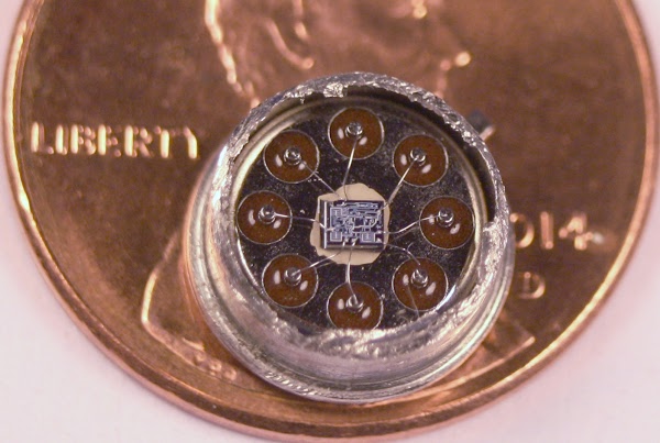
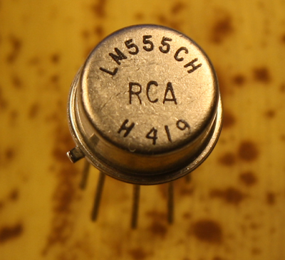
Given the popularity of the 555 timer, I thought it would be interesting to find out what's inside the 555 timer and how it works. While the 555 timer is usually sold as a black plastic IC, it is also available in a metal can, which can be cut open with a hacksaw[3] revealing the tiny die inside.
A brief explanation of the 555 timer
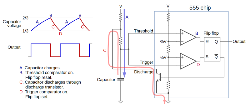
The 555 timer has hundreds of applications, operating as anything from a timer or latch to a voltage-controlled oscillator or modulator. The diagram below illustrates how the 555 timer operates as a simple oscillator. Inside the 555 chip, three resistors form a divider generating references voltages of 1/3 and 2/3 of the supply voltage. The external capacitor will charge and discharge between these limits, producing an oscillation. In more detail, the capacitor will slowly charge (A) through the external resistors until its voltage hits the 2/3 reference. At that point (B), the upper (threshold) comparator switches the flip flop off and the output off. This turns on the discharge transistor, slowly discharging the capacitor (C). When the voltage on the capacitor hits the 1/3 reference (D), the lower (trigger) comparator turns on, setting the flip flop and the output, and the cycle repeats. The values of the resistors and capacitor control the timing, from microseconds to hours.[4]
To summarize, the key components of the 555 timer are the comparators to detect the upper and lower voltage limits, the three-resistor divider to set these limits, and the flip flop to keep track of whether the circuit is charging or discharging. The 555 timer has two other pins (reset and control voltage) that I haven't covered above; they can be used for more complex circuits.
The structure of the integrated circuit
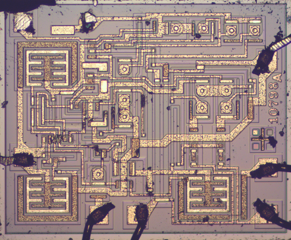
The photo below shows the silicon die of the 555 through a microscope. On top of the silicon, a thin layer of metal connects different parts of the chip. This metal is clearly visible in the photo as yellowish-white traces and regions. Under the metal, a thin, glassy silicon dioxide layer provides insulation between the metal and the silicon, except where contact holes in the silicon dioxide allow the metal to connect to the silicon. At the edge of the chip, thin wires connect the metal pads to the chip's external pins.
The different types of silicon on the chip are harder to see. Regions of the chip are treated (doped) with impurities to change the electrical properties of the silicon. N-type silicon has an excess of electrons (negative), while P-type silicon lacks electrons (positive). In the photo, these regions show up as a slightly different color surrounded by a thin black border. These regions are the building blocks of the chip, forming transistors and resistors.
NPN transistors inside the IC
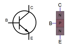
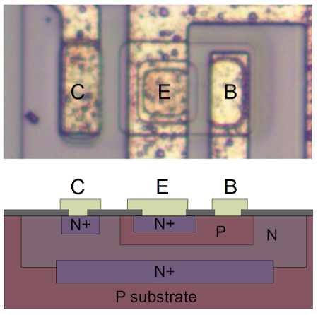
Transistors are the key components in a chip. The 555 timer uses NPN and PNP bipolar transistors. If you've studied electronics, you've probably seen a diagram of an NPN transistor like the one below, showing the collector (C), base (B), and emitter (E) of the transistor, The transistor is illustrated as a sandwich of P silicon in between two symmetric layers of N silicon; the N-P-N layers make an NPN transistor. It turns out that transistors on a chip look nothing like this, and the base often isn't even in the middle!
The photo below shows one of the transistors in the 555 as it appears on the chip. The slightly different tints in the silicon indicate regions that has been doped to form N and P regions. The whitish-yellow areas are the metal layer of the chip on top of the silicon - these form the wires connecting to the collector, emitter, and base. You can spot an emitter on the chip by its "bullseye" structure, while the base rectangle surrounds the emitter.
Underneath the photo is a cross-section drawing illustrating how the transistor is constructed. There's a lot more than just the N-P-N sandwich you see in books, but if you look carefully at the vertical cross section below the 'E', you can find the N-P-N that forms the transistor. The emitter (E) wire is connected to N+ silicon. Below that is a P layer connected to the base contact (B). And below that is an N+ layer connected (indirectly) to the collector (C).[5] The transistor is surrounded by a P+ ring that isolates it from neighboring components.
PNP transistors inside the IC
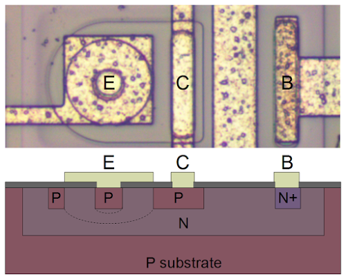
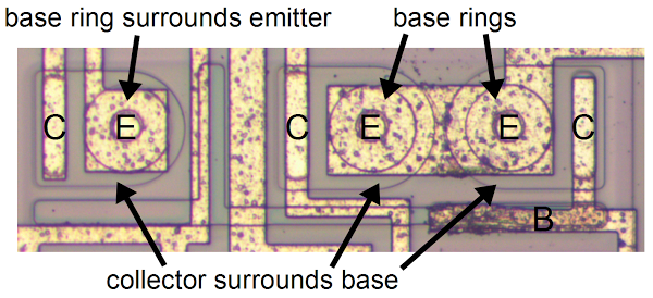
You might expect PNP transistors to be similar to NPN transistors, just swapping the roles of N and P silicon. But for a variety of reasons, PNP transistors have an entirely different construction. They consist of a small circular emitter (P), surrounded by a ring shaped base (N), which is surrounded by the collector (P). This forms a P-N-P sandwich horizontally (laterally), unlike the vertical structure of the NPN transistors.The diagram below shows one of the PNP transistors in the 555, along with a cross-section showing the silicon structure. Note that although the metal contact for the base is on the edge of the transistor, it is electrically connected through the N and N+ regions to its active ring in between the collector and emitter. A metal line is routed between the collector and base, but is not part of the transistor.
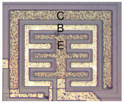
The output transistors in the 555 are much larger than the other transistors and have a different structure in order to produce the high-current output. The photo below shows one of the output transistors. Note the multiple interlocking "fingers" of the emitter and base, surrounded by the large collector.
How resistors are implemented in silicon
Resistors are a key component of analog chips. Unfortunately, resistors in ICs are large and inaccurate; the resistances can vary by 50% from chip to chip. Thus, analog ICs are designed so only the ratio of resistors matters, not the absolute values, since the ratios remain nearly constant.
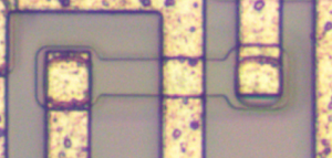
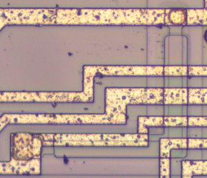
The photo above shows a 1KΩ resistor in the 555, formed from a strip of P silicon (visible as an outline). Note that the resistor connects two metal wires and another metal wire crosses it. The resistor below is an L-shaped 100KΩ pinch resistor. A layer of N silicon on top of the pinch resistor makes the conductive region much thinner (i.e. pinches it), forming a much higher but less accurate resistance.
IC component: The current mirror
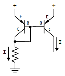
There are some subcircuits that are very common in analog ICs, but may seem mysterious at first. The current mirror is one of these. If you've looked at analog IC block diagrams, you may have seen the symbols below, indicating a current source, and wondered what a current source is and why you'd use one. The idea is you start with one known current and then you can "clone" multiple copies of the current with a simple transistor circuit, the current mirror.
The following circuit shows how a current mirror is implemented with two identical transistors.[6] A reference current passes through the transistor on the left. (In this case, the current is set by the resistor.) Since both transistors have the same emitter voltage and base voltage, they source the same current, so the current on the right matches the reference current on the left.
A common use of a current mirror is to replace resistors. As explained earlier, resistors inside ICs are both inconveniently large and inaccurate. It saves space to use a current mirror instead of a resistor whenever possible. Also, the currents produced by a current mirror are nearly identical, unlike the currents produced by two resistors.
IC component: The differential pair
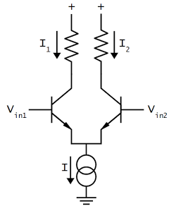
The second important circuit to understand is the differential pair, the most common two-transistor subcircuit used in analog ICs.[7] You may have wondered how a comparator compares two voltages, or an op amp subtracts two voltages. This is the job of the differential pair.
The schematic above shows a simple differential pair. The current sink at the bottom provides a fixed current I, which is split between the two input transistors. If the input voltages are equal, the current will be split equally into the two branches (I1 and I2). If one of the input voltages is a bit higher than the other, the corresponding transistor will conduct more current, so one branch gets more current and the other branch gets less. A small input difference is enough to direct most of the current into the "winning" branch, flipping the comparator on or off.
In the 555, the threshold comparator uses NPN transistors, while the trigger comparator uses PNP transistors. This allows the threshold comparator to work near the supply voltage and the trigger comparator to work near ground. The 555's comparators also use two transistors on each input (Darlington pair) to buffer the inputs.
The 555 schematic interactive explorer
The 555 die photo and schematic[8] below are interactive. Click on a component in the die or schematic, and a brief explanation of the component will be displayed. (For a thorough discussion of how the 555 timer works, see 555 Principles of Operation.)For a quick overview, the large output transistors and discharge transistor are the most obvious features on the die. The threshold comparator consists of Q1 through Q8. The trigger comparator consists of Q10 through Q13, along with current mirror Q9. Q16 and Q17 form the flip flop. The three 5KΩ resistors forming the voltage divider are in the middle of the chip.[9] Urban legend says that the 555 is named after these three 5K resistors, but according to its designer 555 is just an arbitrary number in the 500 chip series
How I photographed the 555 die
Integrated circuit usually come in a black epoxy package which require inconveniently dangerous concentrated acid to open. Instead, I bought a 555 in a metal can (below). To examine the die, I used a metallurgical microscope. Unlike a standard microscope, the metallurgical microscope shines light down through the lens allowing it to work with opaque objects (such as chips). I stitched the photos together with Hugin (details).
The failed improved 555
Given the popularity of the 555, it's surprising that it has several rookie design flaws; unbalanced comparators, large operating currents, an asymmetric output waveform, and temperature sensitivity.[10]In 1997, Camenzind redesigned the 555 to create a much better chip that could run at much lower voltages. The improved chip was sold by Zetex as the ZSCT1555, but unfortunately was a flop. The continuing success of the original 555 and the failure of the improved successor can be viewed as an example of the worse is better principle.
Conclusion
I hope you've found this look inside the 555 timer chip interesting. Next time you're building a 555 project, you'll know exactly what's inside the chip. If you enjoyed this article, I've also reverse-engineered the 741 op amp and 7805 voltage regulator. Thanks to Eric Schlaepfer[11] for helpful comments.Follow me on Twitter and you won't miss an article!
Notes and references
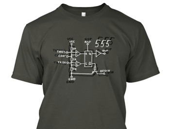
[1] The 555 timer is iconic enough to appear on mugs, bags, caps and t-shirts.
[2] The book Designing Analog Chips written by the 555's inventor Hans Camenzind is really interesting, and I recommend it if you want to know how analog chips work. Chapter 11 has an extensive discussion of the 555's history and operation. Page 11-3 claims the 555 has been the best-selling IC every year, although I don't know if that is still true. The free PDF is here or get the book.
[3] You can cut an IC can open with a plain hacksaw, but a jeweler's saw gives a much cleaner cut. I got a jeweler's saw on eBay for $14, and used the #2 blade. Make sure you cut near the top of the IC so you don't hit the die as I did.
[4] The brilliant part of the 555 timer is that the oscillation frequency depends only on the external resistors and capacitor and is insensitive to the supply voltage. If the supply voltage drops, the 1/3 and 2/3 references drop too, so you might expect the oscillations to be faster. But the lower voltage charges the capacitor more slowly, canceling this out and keeping the frequency constant.
This voltage insensitivity is so tricky that the chip's designer didn't figure it out until near the end of the 555's design, but it made a big difference. The original design was more complex and required nine pins, which is a terrible size for an IC since there are no packages between 8 and 14 pins. The final, simpler 555 design worked with 8 pins, making the chip's packaging much cheaper. (See page 11-3 of Designing Analog Chips for the full story.)
[5] You might have wondered why there is a distinction between the collector and emitter of a transistor, when the typical diagram of a transistor is symmetrical. As you can see from the die photo, the collector and emitter are very different in a real transistor. In addition to the very large size difference, the silicon doping is different. The result is a transistor will have poor gain if the collector and emitter are swapped.
[6] For more information about current mirrors, check wikipedia, any analog IC book, or chapter 3 of Designing Analog Chips.
[7] Differential pairs are also called long-tailed pairs. According to Analysis and Design of Analog Integrated Circuits differential pairs are "perhaps the most widely used two-transistor subcircuits in monolithic analog circuits." (p214) For more information about differential pairs, see wikipedia, any analog IC book, or chapter 4 of Designing Analog Chips.
[8] The 555 schematic used in this article is from the Philips datasheet.
[9] Note that the three resistors for the voltage divider are parallel and next to each other. This helps ensure they have the same resistance even if there are electrical variations across the silicon.
[10] I'm not criticizing the 555; Hans Camenzind points out the design flaws and attributes them to "the early period of IC design (and the inexperience of a rookie designer)"; see Designing Analog Chips, page 11-4. The design of a 555 replacement is discussed in detail in "Redesigning the old 555", IEEE Spectrum, September 1997. That article makes it clear how much much faster IC design is now than in 1970. It took months to create the layout of the 555 chip by hand and manually verify it for correctness. The new chip took two days to layout and 20 minutes to verify.
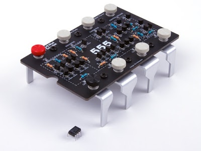
[11] Evil Mad Scientist sells a very cool discrete 555 timer kit, duplicating the 555 circuit on a larger scale with individual transistors and resistors — it actually works as a 555 replacement. Their 555 footstool is also worth a look.

21 comments:
Excellent work Ken! Have been using the 555 for 25 years now. Always wondered how it looked like inside :)
Great article - I enjoyed it.
Slight editing error (I presume) where you state:
"Given the popularity of the 555, it's surprising that it has several rookie design flaws: According to its designer, it has several rookie design flaws:"
Nice article! Good to know the early times of IC design!
very interesting!
as for: "The continuing success of the original 555 and the failure of the improved successor can be viewed as an example of the worse is better principle."
I would attribute this failure to poor marketing. The fact is that modern CMOS version of the 555 are successfull.
Hi,
I'm glad to see some analog IC reverse engineering stuff.
Last year, i tried to reverse the ne556 (there is a nice picture of it from zeptobar: http://zeptobars.com/en/read/stm-ne556-555) and i wasnt able to identify transistor type (pnp/npn). I had no clue for that, so i just ignored the type then tried to eliminate the "impossibru" design with hypothesis (yeah, painful).
As far as i known the circular shape of emitter is for compensating device mismatch between transistors. NPN can also have circular emitter. Or am i wrong?
Btw, the device layout of Q21 looks like a diode?
For me, this shit looks like that
Cool!
I haven't used an actual 555 in a long time; nowadays, in the interest of reduced component count and board space, I end up sending a cheap little MCU to do a 555's job (well, a 555 or maybe a 556 plus passives plus a couple of gates).
Downside of the MCU: with a real analog timer and discrete gates, I'd never have to wonder where-the-heck that stray trailing pulse is coming from. Or, worst case, I could probe the workings with a scope and see what was happening.
useful and interesting for any student from computer engineering or electronics, for high school only at geeks and hackers section
"bite": on the chips I've seen, NPN transistors are usually rectangular and PNP are usually round, because NPN transistors are vertical while PNP transistors are lateral with the base and collector surrounding the emitter. (I'm using "The Art of Analog Layout" page 80 as a reference.) But I don't know if that's true in the 556 you're looking at.
As for Q21, yes it looks like a diode. This is one of the components I puzzled over for a while, since a diode doesn't make sense in the circuit but there's not obvious collector. After looking closely, I think what's happening is there's no isolation "moat" between Q21 and Q22 so they share the same N region connected to Vcc. In other words, Q22's Vcc-to-collector connection also serves as Q21's Vcc-to-collector connection.
Folks at Zeptobars posted nice hi-res die-shot of 555 http://zeptobars.com/en/read/national-semiconductor-LMC555
Probably inspired by your excellent write-up. Thanks!.
@KenShirriff: oh ok right. But you point out another question I always had. Sometimes the N-region (or epitaxial layer) is polarized, in this circuit the whole resistors share the same N-region with Q22 and Q21. What's the purpose of this? For the resistors it's ok, it will reverse bias parasitic diodes but about q22/q21, i have no idea :(
Your book looks like good but a bit expensive :D
My ref. is currently "Bipolar and MOS Analog Circuit Design", it's not bad, I didn't found a better one.
Hi bite, thanks for the comment. I don't know why the resistors and Q21/Q22 share the N region. Maybe it was convenient for layout? Thanks for your book recommendation - I'll take a look. By the way, Amazon has a used copy of "The Art of Analog Layout" for $13.88.
Excellent work mate, so glad I found this site! Thank you for the hard work involved in making such a great page. Don't worry I won't be pointing out what I "think" is an "editing error".
Lmao... I often wonder what needs to happen in someones life to make them do foolish things to someone they have never even met....
Thanks again!!
Wonderful stuff. I am old enough to remember its introduction and have used it many times in my designs over the years. Also fallen into the "crowbar" trap presented with the bipolar versions, especially when working within circuits containing counters or processors etc. where without adequate precautions the 555 will present a microscopic short on the supply rails at switch over and create havoc. Also found it useful as an auto reset device for remote processor based systems (by remote I mean physically remote as in some weather stations) If you gate the address / data lines into a 555 configured as a "missing pulse detector" then should the system freeze, the output of the 555 can be used to perform a reset hopefully restoring function to the system.
This is an amazing website. The interactive die and schematic was my personal favorite. I teach semiconductor fab and packaging classes (die attach and wire bonding) at Lorain County Community College in Elyria, OH and we use the 555 for so many circuits. It's such a versatile circuit. Thank you for putting this together. I will be sharing this with my current classes and my remaining classes as long as it's online. Many thanks and cheers. ~Johnny Vanderford [email protected] www.lcccmems.com
I have done a lot of pictures of different 555 dies.
If you are interested: www.richis-lab.de/555.htm
The comments are in german language but google translator is your friend and of course the pictures are international! :)
One of the best famous IC of the world. Still in use.
I do remember time when 555 was too expensive and exotic for everyday use. There was standard way to implement same functionality with NANDs using all the gates in SN7400, but cannot find it now in the Interwebbs. Especially when Russians started to make 7400 look-a-likes with 2 millimeter pin spacing.
50 years, you can still buy and use it these days!
I joined Magic Dot around 1972 and we were using a modified 555 for our touch switch that Hans had changed the top metal layer for our needs. I met with him later as we were designing an IC for an encoded keyboard version. I believe I still have a wafer of the 555 or the modified version that we used.
Check out these Quantum diamond microscope images of the same die:
https://arxiv.org/pdf/2109.11473.pdf
Hello. I'm confused about Q23. In the schematic it shows it as a diode formed from B to C. Does this mean that it's an NPN with the emitter floating? I can't tell from the die what this structure is. It's also confusing because in Camenzind's book he shows Q23 as a typical diode connected PNP transistor. He also has R10 as 15K instead of 82K. Is there any way to tell from the die any of this stuff? Thanks for the article, by the way. Amazing work.
Post a Comment