The ARM1 chip is the ancestor of the extremely popular ARM processors used in most smart phones. The ARM1 is a good choice for reverse engineering since it was designed in 1985 and its simple RISC silicon circuits are easier to understand than modern processors. This article jumps into the chip details; if you want an overview of the ARM1 internals, start with my first article on reverse engineering the ARM1.
The priority encoder takes a 16-bit binary field, finds the bits that are set and outputs the 4-bit binary positions of these bits in sequence. For example, if the input field is 1000000000001011, successive outputs will be 0, 1, 3, and 15. (Bits are scanned starting with bit 0, the rightmost bit.) The priority encoder gets its name because it selects bits by priority (rightmost first) and encodes the result into binary.
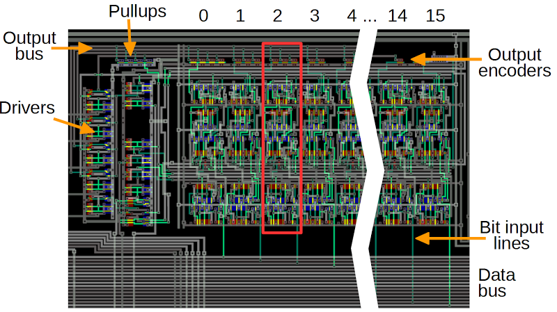
The diagram below shows the layout of the priority encoder on the chip. It is implemented as 16 bit slices, one for each bit, arranged left to right ("backwards"). Slice 2 is highlighted in red; slices 5 through 13 have been cut out to make the image fit. The 16 input bits arrive through the data bus on the bottom and each bit enters a slice through one of the bit input lines (green). If the bit is currently the highest priority, the output encoder at the top of the slice generates the 4-bit binary value on the output bus. The pullups pull the output bus lines to the high state. Finally, the drivers amplify the output signals and send them to other parts of the chip.[1]
The priority encoder is a key part of the ARM processor's block data transfer instructions, which efficiently copy data between on-chip registers and memory storage.[2] These instructions can transfer any subset of ARM's 16 registers in a single instruction. The desired registers are specified by setting the corresponding bits in a 16-bit field in the instruction. The role of the priority encoder is to scan this field and determine which register to transfer during each step of the operation.
Implementation of the priority encoder
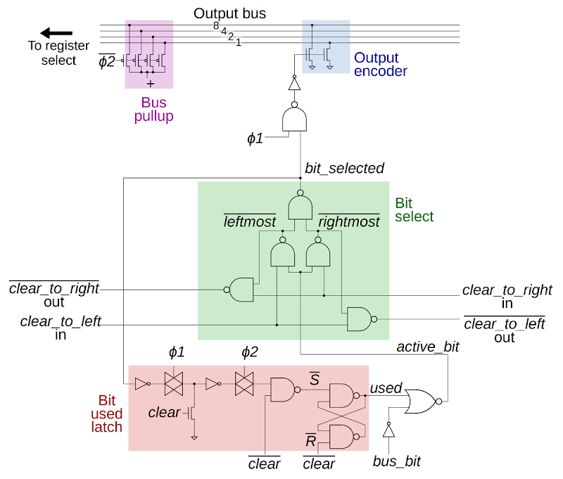
The schematic below shows one of the 16 slices in the priority encoder. The input bit from the bus, bus_bit enters at the bottom. The green bit select block determines if the bit is currently the high-priority bit. If so, bit_selected becomes 1. The output encoder (blue) puts the binary value associated with the selected bit onto the bus. Finally, the bit used latch (red) marks the bit as used, blocking it and allowing the next bit in sequence to be active in the next cycle. The two-phase clock signals Φ1 and Φ2 cause the priority encoder to move from bit to bit.
The bit selection logic (green) is fairly straightforward. The input clear_to_left is 1 if all the bits to the left are clear. If all the bits to the left are clear and the current bit is set, then this bit is selected by the priority encoder. This also blocks clear_to_left from being passed to the next slice. Otherwise, clear_to_left is passed along. Thus, as it passes through the circuit clear_to_left will be 1 until a bit is encountered, and then 0 from that point. If the final clear_to_left output is 1, then all bits are clear and encoding is done. The logic for clear_to_right is similar, allowing the highest-priority bit to be selected from the right instead. Normally the initial clear_to_left input is 0, and the initial clear_to_right bit is 1, enabling the left scan and disabling the right scan.
The bit used latch (red) keeps track of which bits have already been output. It is what allows the priority encoder to move from bit to bit each clock cycle. The two transmission gates (indicated with the four-triangle symbol) are clocked alternately so the bit_selected signal will move through the circuit after two half-clocks. Two NAND gates are connected as an SR latch to store this signal. Once a slice has selected a bit, the latch remembers that the bit has been used and blocks bus_bit from flowing into the bit select circuit. This allows the next bit in sequence to be selected. The bit used circuit also has a clear signal that resets the latch for a new instruction.
The bus pullup circuit (purple) and the output encoder (blue) work together to output the binary value corresponding to the selected bit. They use dynamic logic rather than standard gates to reduce the circuit size. This logic depends on the clock and the capacitance of the output bus lines to generate the right values. In phase 2 of the clock, the bus pullup transistors pull the output bus lines high. Then, in phase 1, the output encoder in the active slice pulls the appropriate lines low so the bus will have the correct value. The schematic above shows the encoder for slice 6: the transistors attached to lines 8 and 1 pull them low, leaving 4 and 2 high; the resulting binary 0110 is 6. One set of pullup transistors supports the whole priority encoder, while each slice has its own output encoder transistors.
The output bus lines pass through drivers to boost the current; the signal on the output bus is relatively weak since it is generated by dynamic logic. The output flows to the register select circuit to select the appropriate register for the data transfer. See Dave Mugridge's article on ARM1 register selection for details on how registers are selected.
Discussion
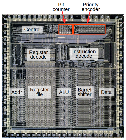
The block data move transfer instructions in the ARM1 require two special functional units: the priority encoder and the bit counter (which I reverse-engineered earlier). These two circuits are highlighted in red in the ARM1 die photo below. Supporting block data transfers added significant complexity to the chip (about 3% by area), but the chip designers felt the performance gain from block transfers was worth it.
One interesting thing about the priority encoder's design is alternating slices have inverted logic: NAND gates become NOR gates and vice versa. The reason is to avoid inverters between stages. You'll note on the schematic that the clear_to_right and clear_to_left outputs are inverted. The obvious design would add inverters to fix the polarity. However, this would add an extra gate delay in each stage, which is significant when the signal has to ripple through 16 stages. By "flipping" alternate stages, this delay is avoided. The trick of alternating stages to avoid inverters is used in other chips. For example, the 8085's incrementer and the 6502's ALU.
One surprise with the ARM1 priority encoder is it supports both low-to-high priority and high-to-low priority, but high-to-low priority is disabled and not used. That is, the rightmost clear_to_right is wired to 1, so the rightmost bit circuitry will never be active. The explanation for this unused circuitry is interesting.
When using the block data operations to push and pull registers on the stack, you'd expect to push R0, R1, R2, etc and then pop in the reverse order R2, R1, R0.[3] To handle this, the priority encoder needs to provide the registers in either order, and the address incrementer needs to increment or decrement addresses depending on whether you're pushing or popping, and the chip includes this circuitry. However, there's a flaw that wasn't discovered until midway through the design of the ARM1. Register 15 (the program counter) must always be updated last, or else you can't recover from a fault during the instruction because you've lost the address.[4]
The solution used in the ARM1 is to always read or write registers starting with the lowest register and the lowest address. In other words, to pop R2, R1, R0, the ARM1 jumps into the middle of the stack and pops R0, R1, R2 in the reverse order. It sounds crazy but it works. (The bit counter determines how many words to shift the starting position.) The consequence of this redesign was that the circuitry to decrement addresses and priority encode in reverse order is never used. This circuity was removed from the ARM2.
Conclusion
The priority encoder is a large functional unit in the ARM1 chip, used for the block data transfer instructions. By looking at one of the 16 slices in the encoder, the circuit can be reverse-engineered and understood. While largely built from standard logic gates, the circuit also uses transmission gates and dynamic logic for efficiency. One surprise is the priority encoder contains unused logic allowing it to work in either direction. This wasted circuitry is left over from a design change during the development of the ARM1.Now that you've seen the internals of the priority encoder, you can use the Visual ARM1 simulator to see the circuit in action.[5]
Notes and references
[1] The drivers also invert and buffer clock signals that are used by the priority encoder.[2] ARM's block data transfer instructions are called STM (Store Multiple) and LDM (Load Multiple), storing and loading multiple registers with one instruction. These instructions can be used for copying data or for stack push/pop, saving registers in a subroutine call or interrupt handler. Note that these instructions are not implemented in microcode, but in hardware that steps through the registers and memory. These instruction are explained in detail on the ARMwiki.
[3] The block data transfer instructions work for general register copying, not just pushing and popping to a stack. It's simpler to explain the instructions in terms of a stack, though.
[4] If an instruction encounters a memory fault (e.g. a virtual memory page is missing), you want to take an interrupt, fix the problem (e.g. load in the page), and then restart the instruction. However, if you update registers high-to-low, R15 (the program counter) will be updated first. If a fault happens during the instruction, the address of the instruction (R15) is lost, and restarting the instruction is a problem.
One solution would be to push registers high-to-low and pop low-to-high so R15 is always updated last. Apparently the ARM designers wanted the low register at the low address, even if the stack grows upwards, so popping R15 least wouldn't work. Another alternative is to have a "shadow" program counter that can restore the program counter during a fault. The ARM1 designers considered this alternative too complex. For details, see page 248 of "VLSI RISC Architecture and Organization", by Stephen Furber, one of the ARM1's designers.
[5] Thanks to the Visual 6502 team for providing the simulator and ARM1 chip layout data. If you're interested in ARM1 internals, also see Dave Mugridge's series of posts.


No comments:
Post a Comment