ARM is now the world's most popular instruction set but it has humble beginnings. The original ARM1 processor was designed in 1985 by a UK company called Acorn Computer for the BBC Micro home/educational computer. A few years later Apple needed a low-power, high-performance processor for its ill-fated Newton handheld system and chose ARM.[1] In 1990, Acorn Computers, Apple, and chip manufacturer VLSI Technology formed the company Advanced RISC Machines to continue ARM development. ARM became very popular for low power applications (such as phones) and now more than 50 billion ARM processors have been manufactured.
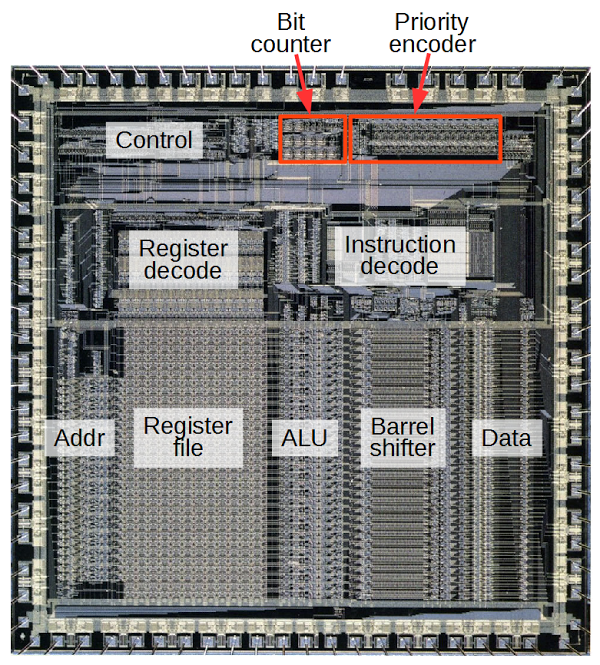
One way ARM processors increase performance is through block data transfer instructions, which efficiently copy data between on-chip registers and memory storage.[2] These instructions can transfer any subset of ARM's 16 registers in a single instruction. The desired registers are specified by setting the corresponding bits in a 16-bit field in the instruction. To implement the block transfer instructions, the ARM requires two specialized circuits. The first circuit, the bit counter, counts the number of bits set in the register select field to determine how many registers are being transferred.[3] The second circuit, the priority encoder, scans the register select field and finds the next set bit, indicating which register to load/store next.
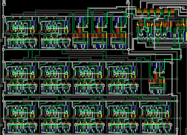
Zooming in on the bit counter reveals the circuit below. It looks like a jumble of lines, but by examining it carefully, you can get an understanding of what is going on. The remainder of the article explains how a special type of circuitry called pass transistor logic is used to build a multiplexer — a circuit that selects one of its two inputs. The multiplexers are used to form logic gates, which are then combined to form a full adder, which adds three bits. Finally, the adders are combined to create the bit counting circuit. If you're not familiar with digital logic or the ARM processor, you might want to start with my earlier article on reverse-engineering the ARM1 for an overview.
Pass transistors and transmission gates
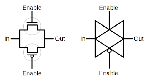
The bit counter is built from a type of circuitry called pass transistor logic. Unlike normal logic gates, pass transistor logic switches the inputs themselves to pass an input directly to the output. Pass transistors are used because sums (i.e. XORs) are inconvenient to generate with standard logic and can be generated more efficiently with pass transistor logic.The ARM1 chip, like most modern chips, is built from a technology called CMOS. The C in CMOS stands for complementary because CMOS circuits are built from two complementary types of transistors. NMOS transistors switch on when the control signal on the gate is high, and can pull the output low. PMOS transistors are opposite; they switch on when the gate's control signal is low, and can pull the output high. Combining an NMOS transistor and a PMOS transistor in parallel forms a transmission gate. If both transistors are on, the input will be passed to the output whether it is low or high. If both transistors are off, the input is blocked. Thus, the circuit acts as a switch that can either pass the input through to the output or block it.
The diagram below shows two transistors (circled) connected to form a transmission gate. The upper one is NMOS and the lower one is PMOS. On the right is the symbol for a transmission gate. Note that because the transistors are complementary, they require opposite enable signals.
The multiplexer
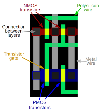
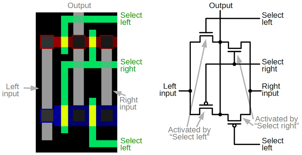
Next, we can look at how transmission gates are used in the chip. The diagram below shows a multiplexer as it appears in the Visual ARM1 simulator. The ARM1 chip is constructed from five layers, which appear as different colors in the simulator. (The layers are harder to distinguish in the real chip.) The bottom layer is the silicon that makes up the transistors of the chip. During manufacturing, regions of the silicon are modified (doped) by applying different impurities. Silicon can be doped positive to form a PMOS transistor (blue) or doped negative for an NMOS transistor (red). Undoped silicon (black) is basically an insulator. Polysilicon wires (green) are deposited on top of the silicon. When polysilicon crosses doped silicon, it forms the gate of a transistor (yellow). Finally, two layers of metal[4] (gray) are on top of the polysilicon and provide wiring. Black squares are contacts that form connections between the different layers.
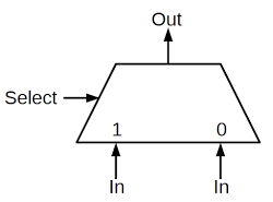
Each multiplexer consists of four transistors: two NMOS (red) and two PMOS (blue); the gate appears in yellow between the two sides of the transistor. These form two transmission gates allowing either the left input or the right input to be connected to the output. If "Select left" is high and "Select right" is low, the two transistors on the left turn on, connecting the left input to the output. Conversely, if "Select right" is high and "Select left" is low, the two transistors on the right turn on, connecting the right input to the output.
Building a full adder from multiplexers
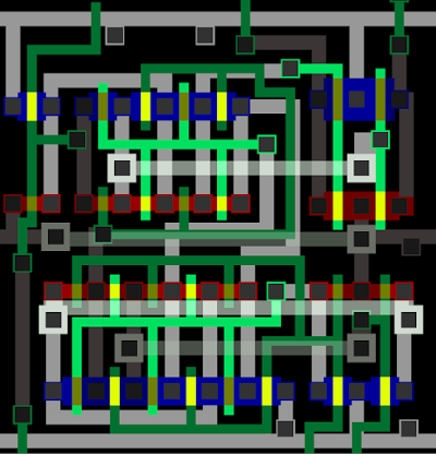
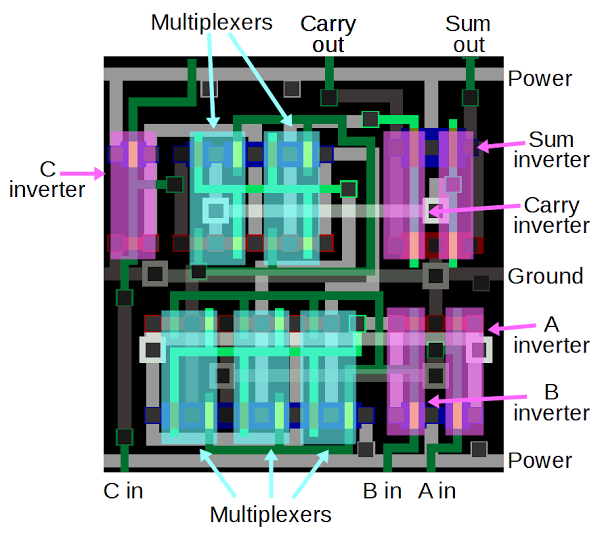
A full adder is a digital circuit to add two bits along with a carry in, generating a sum output and a carry output. (If you think of the output as a binary sum, the sum output is the low bit and the carry output is the high bit.) Equivalently, the full adder can be thought of as adding three input bits. The full adder is the building block of the ARM1's bit counting circuit.In the ARM1, a full adder is built from multiplexers, along with a few inverters. The diagram below shows how a full adder appears in the simulator. Counting the yellow rectangles, you can see that there are 29 transistors in the circuit. The transistors are connected by metal wires (gray) and polysilicon wires (green). While the layout may appear chaotic, the transistors are arranged in an orderly way: a row of PMOS transistors (blue), two rows of NMOS transistors (red), and a second row of PMOS transistors (blue).[5]
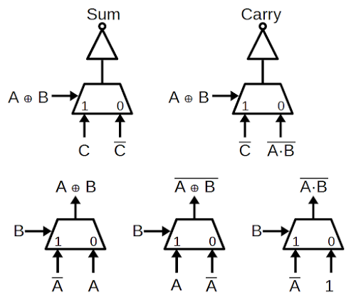
The schematic below shows how the full adder in the ARM1 is built from multiplexers. In the lower left, a multiplexer generates "A XOR B", which is the single-bit sum of A and B. If you try the combinations of A and B, you'll find that the output is 1 if exactly one of the inputs is 1, and otherwise 0. The next multiplexer reverses the A inputs and computes the complement of A XOR B.[6] The third multiplexer implements a NAND gate: If B is 1 and A is 1, the output is 0.[7]
The multiplexers in the upper half compute the sum and carry (i.e. bit 0 and bit 1 of the binary sum), as can be verified by trying the input combinations. You might wonder why inverters are used, rather than generating the desired outputs directly. The reason is to boost the signals, since the outputs of multiplexers are relatively weak.
The diagram below indicates the multiplexers and inverters[6] that make up a full adder, with the components highlighted. Each multiplexer is built as described earlier, and they are arranged as in the schematic above. The multiplexers are connected together by polysilicon and metal wires. The three inputs are at the bottom and the two outputs are at the top. This adder is the main block used to build the bit counter, and the next section will show how adders are connected together.
Building the bit counter from adders
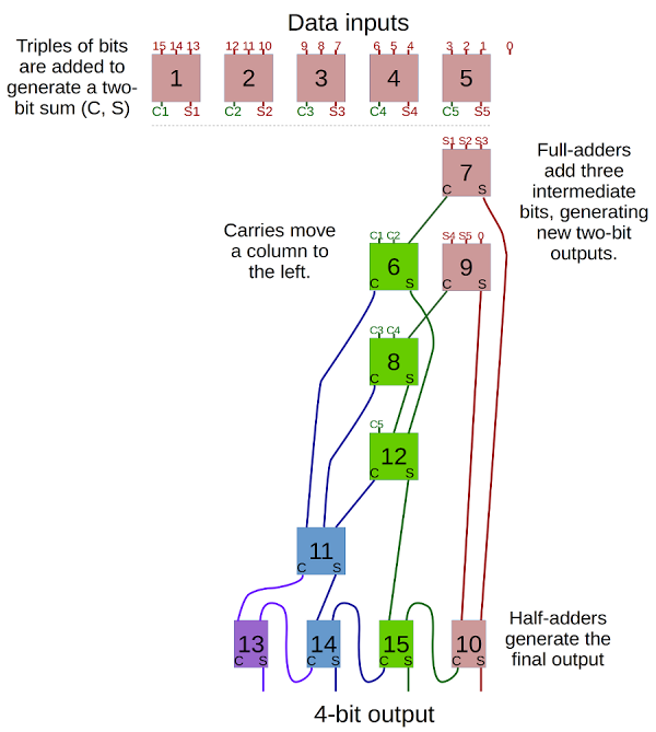
The bit counter takes 16 bit inputs and generates a 4-bit count as output, using adders as building blocks. The flow chart below shows how it operates, with data flowing from top to bottom. Each box is an adder, with carry (C) and sum (S) outputs. Boxes are colored according to which bit of the sum they are computing: red for the 1's bit, green for the 2's bit, blue for the 4's bit and purple for the 8's bit. Each box passes its sum output down and passes its carry to the left.Overall, the process is similar to long addition if you could just add three digits at a time. You compute partial sums, then add up those sums, and so forth until all the sums are added up. Then the carries need to be added up, along with the sums of those carries, and so forth. If there are carries from those digits, they need to be added up, until finally everything has been added.
The first step of counting the bits is to add each triple of bits with a full adder, generating a two bit count (0, 1, or 2). Inconveniently, since the sixteen input bits aren't divisible by 3, one bit is left over and is handled separately. Next, the five partial sums are added by more adders (red). As carries are generated, they also get added (green). Carries from the carries are also added (blue). In the final step, two-input half adders[8] compute the sum output; these half adders are simpler than the three-input full adders.[9]
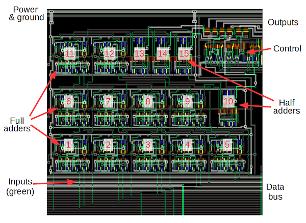
The diagram below shows how the flow chart above is implemented on the chip to create the entire bit counter circuit. The adders are numbered to match the flow chart. The data bus is at the bottom, connected to the bit counter inputs by 16 polysilicon wires (green). Data flows generally upwards through the circuit, opposite to the flow chart. The five adders at the bottom add triples of input bits, and the remaining adders combine the sums and carries. The four half adders are connected to the output drivers in the upper right. The control circuit enables and disables the output drivers, so the bit count is output to the bus at the right times.
Conclusion
Well, it's been quite a journey from individual transistors to the bit counter, a complex functional block in a real processor. Hopefully this article has taken some of the mystery out of how circuits in a processor are constructed. Now you can try out the Visual ARM1 simulator and take a look at this circuit in action.[10]Notes and references
[1] An interesting interview with Steve Furber, co-designer of the ARM1, explains how ARM achieved low power consumption. Acorn wanted to use a low-cost plastic package for the chip, but it could only handle 1 Watt. The designers didn't have good tools for estimating power consumption, so they were conservative in their design and the final power consumption was way below the target, just 1/10 Watt. In addition, ARM1 had a simple RISC (Reduced Instruction Set Computer) design, which also reduced power consumption: ARM1 had about 25,000 transistors compared to 275,000 in the 80386 which came out the same year. Thus, the low power consumption of ARM that led to its wild success in mobile applications was largely accidental.[2] ARM's block data transfer instructions are called STM (Store Multiple) and LDM (Load Multiple), storing and loading multiple registers with one instruction. These instructions don't exactly fit the RISC processor philosophy since they are fairly complex and perform many memory accesses, but the ARM designers took the pragmatic approach and implemented them for efficiency. These instructions can be used for copying data or for stack push/pop, saving registers in a subroutine call or interrupt handler. Note that these instructions are not implemented in microcode, but in hardware that steps through the registers and memory.
[3] It's not obvious why a bit counter is required at all. You'd think the chip could just store registers until it's done, without knowing the total count. The unexpected answer is that LDM/STM always start with the lowest address working upwards. For example, if you're popping 4 registers off the stack with LDM, you'd expect to start at the top of the stack and work down. Instead, the ARM pulls registers out of the middle of the stack: it starts four words from the top, pops registers in reverse order going up, and then updates the stack pointer to the bottom. The results are exactly the same as popping from the top, just the memory accesses are in the reverse order. (The STM instruction is explained in detail on the ARMwiki.) Thus, the bit counter is needed to figure out how far down to jump in memory at the start of the instruction.
That raises the question of why would memory accesses always go low to high, even when that seems backwards. The explanation is that you want to update register 15 (the program counter) last, so if there's a fault during the instruction you haven't clobbered the instruction address and can restart. This problem was discovered partway through the ARM1 design, causing the designers to implement the new strategy that block transfers always go from lowest register to highest register and lowest address to highest address. The bit counter was added to support this. Some remnants of the earlier, simpler design are visible in the ARM1. Specifically, the priority encoder can operate either direction, but high-to-low is never used. In addition, the address incrementer can both increment and decrement addresses, but decrement is never used. The unused circuitry was removed from the later ARM2.
[4] At the time, having two layers of metal in the chip instead of one was a risky technology. However, the ARM1 designers wanted the convenience of two layers, which made routing the chip much simpler.
[5] A few other things to point out in the multiplexer layout. Note that the second input to each multiplexer matches the first input to the next multiplexer. This lets neighboring multiplexers share inputs, so they can be packed together more closely. Another thing of interest is the transistor sizes. The PMOS transistors are about twice the size of the NMOS transistors in order to provide the same current. The reason is that electrons carry the charge around in NMOS transistors, while "holes" carry the charge in PMOS transistor, and electrons move faster, providing more current (details). Finally, the transistors in the upper right are larger. These transistor drive the outputs from the multiplexer, so they must provide more current.
[6] You might wonder why the circuit computes the complement of A XOR B when it isn't used in the schematic. The reason is the multiplexer uses both the select input and the complement of the select input. Thus, the complement is used; it just isn't explicitly shown in the schematic. Likewise an inverter complements B, so it is available for the select lines.
[7] It is very unusual to implement a NAND gate with a multiplexer. Normally CMOS circuits implement a NAND gate with a standard four transistor circuit. But since the circuit already had multiplexers, adding an additional one was more efficient than the standard NAND gate.
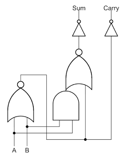
[8] The half adder is built from standard gates, rather than multiplexers, as shown in the schematic below. The half adder's behavior is different from a standard half adder: it computes A+B+1 instead of A+B. Thus, the output of the four half adders is equivalent to adding binary 1111 to the sum, equivalent to subtracting 1. The output drivers invert this, so the output on the bus is the twos complement of the sum. The outputs are also shifted two bits on the bus, multiplying the value by 4 (since ARM registers are 4 bytes long). For example, if you pop 3 registers the stack will be decremented by 12 bytes.
[9] The circuit complexity of the bit counter is interesting. To sum 16 bits requires 15 adders. In general, summing N bits will require N-1 adders (for N a power of 2). Note that each adder takes 3 lines down to 2, so reducing N lines down to 1output requires N-1 adders. (There are 4 outputs, not 1, but the half adders bump the total back to N-1). The number of adders for each output bit is a power of 2: 1 purple, 2 blue, 4 green, 8 red. Larger sum circuits could be created by combining two smaller ones. For example, two 16-bit counter circuits could be combined to create a 32-bit counter circuit by adding four more full adders to add the results from each half, before the final half-adder layer. The circuit used in the ARM1 isn't quite the recursive design, pushing more adders to the first layer. An important part of the design is to minimize propagation delay; in the ARM1 design, signals go through 6 adders in worst case, slightly better than the purely recursive design.
[10] Thanks to the Visual 6502 team for providing the simulator and ARM1 chip layout data. If you're interested in ARM1 internals, also see Dave Mugridge's series of posts.

Great article!
ReplyDeleteYou noted that the ARM1 layout is much more regular than say the 6502 or Z-80. I wonder how much of that is because they didn't care as much about area, and how much it is because of the constraints of CMOS design compared to NMOS or PMOS?
I have done some hobby CMOS layout, just to try to get a feel for it (using Magic VLSI, which is free but a bit archaic), and one thing that has struck me is how much you're constrained by the design rule that requires a minimum distance between NMOS and PMOS transistors (i e between N and P diffusion). Maybe it just wasn't possible to create the same kind of jigsaw puzzle layout in CMOS? It would be interesting to compare e g the layout of the 6502 and the 65c02 to see if they managed to squeeze out some of the air in the 65c02 CMOS design as well.