The IBM 1401 computer uses an unusual technique called qui-binary arithmetic to perform arithmetic. In the early 1960s, the IBM 1401 was the most popular computer, used by many businesses for the low monthly price of $2500. For a business computer, error detection was critical: if a company sent out bad payroll checks because of a hardware fault, it would be catastrophic. By using qui-binary arithmetic, the IBM 1401 detects arithmetic errors.
If you've studied digital circuits, you've seen the standard binary adder circuits that add two numbers. But the IBM 1401 uses a totally different approach. Unlike modern computers, the IBM 1401 operates on decimal digits, not binary numbers, using BCD (binary-coded decimal). To add two numbers, digits are converted from BCD to qui-binary, added together with a special qui-binary adder, and then converted back to digits in BCD. This may seem pointlessly complex, but it allows easy error detection.
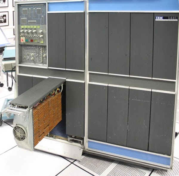
The photo below shows the IBM 1401 with one panel opened to show the addition/subtraction circuitry, made up of dozens of Standard Module System (SMS) cards. Each SMS card holds a simple circuit with a few germanium transistors (the computer predates silicon transistors). This article explains in detail how these circuits implement it.
What is qui-binary?
Qui-binary code is a way of representing a decimal digit with 7 bits. The number is split into a qui part (0, 2, 4, 6, or 8) and a binary part (0 or 1).[1] For example, 3 is split into 2+1, and 8 is split into 8+0. The qui part is labeled Q0, Q2, Q4, Q6, or Q8 and the binary part is B0 or B1. The number is then represented by seven bits: Q8Q6Q4Q2Q0B1B0. The following table summarizes the qui-binary representation.
| Digit | Qui | Binary | Bits: Q8Q6Q4Q2Q0B1B0 |
|---|---|---|---|
| 0 | Q0 | B0 | 0000101 |
| 1 | Q0 | B1 | 0000110 |
| 2 | Q2 | B0 | 0001001 |
| 3 | Q2 | B1 | 0001010 |
| 4 | Q4 | B0 | 0010001 |
| 5 | Q4 | B1 | 0010010 |
| 6 | Q6 | B0 | 0100001 |
| 7 | Q6 | B1 | 0100010 |
| 8 | Q8 | B0 | 1000001 |
| 9 | Q8 | B1 | 1000010 |
The advantage of qui-binary is error detection, since it is straightforward to detect an invalid qui-binary number.[2] A valid qui-binary number has exactly one qui bit and exactly one binary bit. Any other qui-binary number is faulty. For instance, Q4 Q2 B0 is bad, as is Q8. A problem in any bit creates a bad qui-binary number and can be detected.
Overview of the 1401's qui-binary circuit
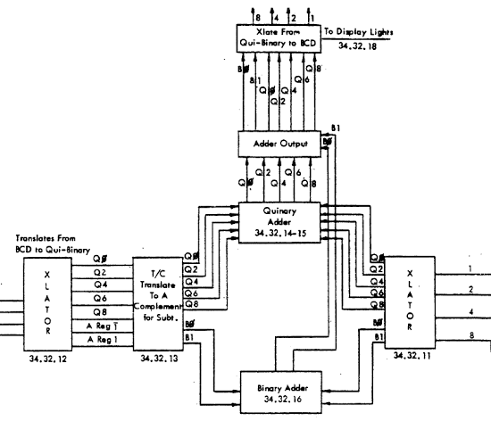
The IBM 1401's arithmetic unit operates on one digit at a time, adding them with a qui-binary adder.[3] The block diagram below[4] shows how the adder takes two binary-coded decimal digits, stored in the A and B temporary registers, and produces their sum. The digit from the A register enters on the left, and is translated to qui-binary by the translation circuit (labeled XLATOR). This qui-binary value goes through a translate/complement circuit which is used for subtraction. The digit in the B register enters on the right and is also converted to qui-binary. The binary bits (B0/B1) are added by the binary adder at the bottom. The quinary values are added with a special quinary adder. The adder output circuit combines the quinary bits with any carry, generating the qui-binary result. Finally, the translation circuit at the top converts the qui-binary result back to a BCD digit, sending the BCD value to core memory and to the console display lights.[5]
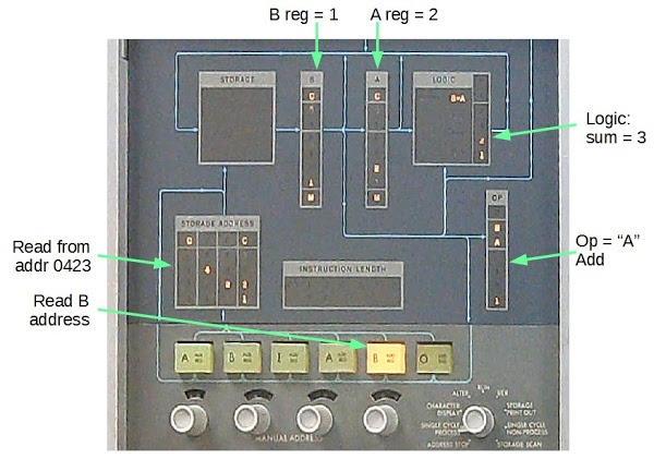
The photo below shows the IBM 1401 console during an addition instruction. The numbers are displayed in binary-coded decimal; the qui-binary representation is entirely hidden from the programmer. At this point in the addition instruction, the digit 1 was read from address 423 into the B register, and is added to the digit 2 already in the A register. The result from the qui-binary adder is 3 (binary 2 + 1), which is stored back to memory.[6]
BCD to qui-binary translation
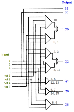
To examine the addition/subtraction circuitry in more detail, we'll start with the logic that converts a BCD digit to qui-binary. The logic is implement with an AND-OR structure that is common in the 1401. Note that the logic gate symbols are different from modern symbols: an AND gate is represented as a triangle, and an OR gate is represented as a semi-circle. Each bit of the BCD digit, as well as the bit's complement, is provided as input. Each AND gate matches a specific bit pattern, and then the results are combined with an OR gate to generate an output.
To see how this works, look at the AND gate at the bottom (labeled 8, 9). Tracing the wires to the inputs, this gate will be active if input 8 AND input not-4 AND input not-2 are set, i.e. if the input is binary 1000 or 1001. Thus, output Q8 will be set if the input digit is 8 or 9, just as required for the qui-binary code.
For a slightly more complicated case, the first AND gate matches binary 1010 (decimal 10), and the second AND gate matches binary 000x (decimal 0 or 1). Thus, Q0 will be set for inputs 0, 1, or 10. Likewise, Q2 is set for inputs 2, 3, or 11. The other Q outputs are simpler, computed with a single AND gate.[7]
The B0 and B1 outputs are simply wires from the not-1 and 1 inputs. If the input is even, B0 is set, and if the input is odd, B1 is set.
9's complement circuit
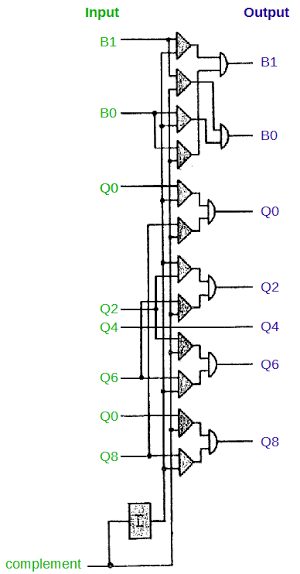
To perform subtraction, the IBM 1401 adds the 9's complement of the digit. The 9's complement is simply 9 minus the digit. The complement circuit below passes the qui-binary number through unchanged for addition or complemented for subtraction.[8] The complement input selects which mode to use; it is generated from the operation (addition or subtraction), and the signs of the input numbers.To see how complementation works in qui-binary, consider 3 (Q2 B1). Its complement is 6 (Q6 B0). The general pattern for complementation is B0 and B1 get swapped. Q0 and Q8 are swapped, and Q2 and Q6 are swapped. Q4 is unchanged; for example, 4 (Q4 B0) is complemented to 5 (Q4 B1).[9]
Quinary adder
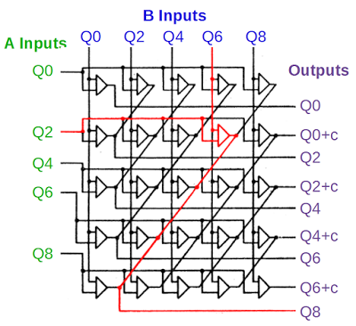
The circuit below adds the quinary parts of the two numbers and can be considered the "meat" of the adder. The qui part from the A register is on the left, the qui part from the B register is on the top, and the qui output is on the right. The outputs with "+c" indicate a carry if the result is 10 or more. The addition logic is implemented with a "brute force" matrix, connecting each pair of inputs to the appropriate output. An example is Q2 + Q6, shown in red. If these two inputs are set, the indicated AND gate will trigger the Q8 output.[10]
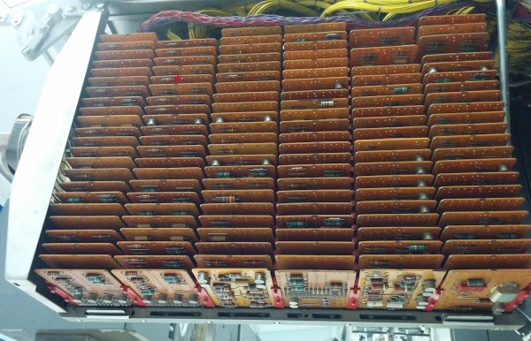
In the photo below, we can find the exact card in the IBM 1401 that performs this addition. The card in the upper left marked with a red asterisk computes the output Q8.[11]
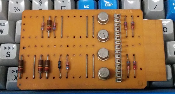
The circuitry in the IBM 1401 is simple enough that you can follow it all the way to the function of individual transistors.[12] The asterisk-marked card is a 3JMX SMS card containing 4 AND gates, and is shown below. Each of the round metal transistors corresponds to one AND gate for one of the sums that generates the output Q8. The top transistor is activated by inputs 8+0, the next for 0+8, the next 6+2, and the bottom one 2+6. Thus, the bottom transistor corresponds to the red AND gate in the schematic above.[13]
Qui-binary to BCD translation
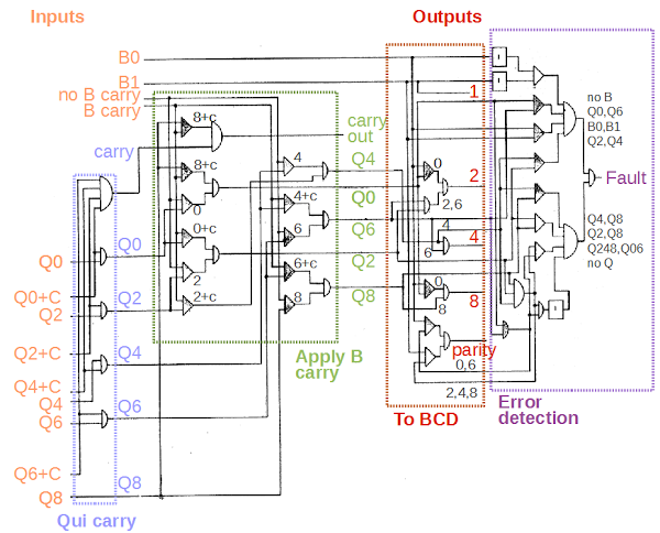
The diagram below shows the remainder of the qui-binary adder, which combines the qui and binary parts of the output, converts the output back to BCD, and detects errors. I'll just give an overview here, with more explanation in the footnotes.[14] The qui-binary carry circuit, in the blue box, processes the carry signals from the adder circuit. The next circuit, in the green box, applies any carry from the B bits, incrementing the qui component if necessary. The translation circuit, in red, converts the qui-binary result to BCD, using AND-OR logic. It also generates the parity output used for error detection in memory. The final circuit, in purple, is the error detection circuit which verifies the qui-binary result is valid and halts the computer if there is a fault.
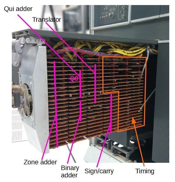
The photo below shows the functions of the different cards in the arithmetic rack.[15] The cards in the left half perform arithmetic operations. Each function takes multiple cards, since a single SMS card has a small amount of circuitry. "Q8" indicates the card discussed earlier that computes Q8. The right half is taken up with clock and timing circuits, which generate the clock signals that control the 1401.
Conclusion
This article has discussed how the 1401 adds or subtracts a single digit. The complete addition/subtraction process in the 1401 is even more complex because the 1401 handles numbers of arbitrary length; the hardware loops over each digit to process the entire numbers.[16][17]Studying old computers such as the IBM 1401 is interesting because they use unusual, forgotten techniques such as qui-binary arithmetic. While qui-binary arithmetic seems strange at first, its error-detection properties made it useful for the IBM 1401. Old computers are also worth studying because their circuitry can be thoroughly understood. After careful examination, you can see how arithmetic, for instance, works, down to the function of individual transistors.
Thanks to the 1401 restoration team and the Computer History Museum for their assistance with this article. The IBM 1401 is regularly demonstrated at the Computer History Museum, usually on Wednesdays and Saturdays (schedule), so check it out if you're in Silicon Valley.
Notes and references
[1] Qui-binary is the opposite of bi-quinay encoding used in abacuses and old computers such as the IBM 650. In bi-quinary, the bi part is 0 or 5, and the quinary part is 0, 1, 2, 3, or 4.[2] You might wonder why IBM didn't just use parity instead of qui-binary numbers. While parity detects bit errors, it doesn't work well for detecting errors during addition. There's no easy way to figure out what the parity should be for a sum.
[3] The IBM 1401 has hardware to multiply and divide numbers of arbitrary length. The multiplication and division operations are based on repeated addition and subtraction, so they use the qui-binary addition circuit, along with qui-binary doublers.
[4] The logic diagrams are all from the 1401 Instructional Logic Diagrams (ILD). Pages 25 and 26 show the addition and subtraction logic if you want to see the diagrams in context.
[5] The IBM 1401 performs operations on memory locations and the A and B registers provide temporary storage for digits as they are read from core memory. They are not general-purpose registers as in most microprocessors.
[6] A few more details about the console display. The "C" bit at the top of each register is the check (parity) bit used for error detection. The 1401 uses odd parity, so if an even number of bits are set, the C bit is also set. The "M" bit at the bottom is the word mark, which indicates the end of a variable-length field. The machine opcode character is zone B + zone A + 1, which indicates the letter "A".
Unlike modern computers, the 1401 uses intuitive opcodes so "A" means add, "S" means subtract, "B" means branch and so forth. (This is the actual opcode in memory, not the assembly mnemonic.) In the lower right, the mode knob is set to "Single cycle process", which allowed me to step through the instruction to get this picture. Normally this knob is set to "Run" and the console flashes frantically as instructions are executed.
[7] One surprising feature of the BCD translator is that it accepts binary inputs from 0 to 15, not just "valid" inputs 0 to 9. Input 10 is treated as 0, since the 1401 stores the digit 0 as decimal 10 in core. Values 11 through 15 are treated as 3 through 7. Thus, every binary input results in a valid (but probably unexpected) qui-binary value. As a result, the 1401 can perform addition on non-decimal characters, but the results aren't very useful.
[8] The IBM 1401 uses 9's complements since it is a decimal machine, unlike modern binary computers which use 2's complements. For example, the complement of 1 is 8, and the complement of 4 is 5. To subtract a number, the 9's complement of each digit is added (along with a carry). An example of using complements for subtration is 432 - 145. The 9's complement of 145 is 854. 432 + 854 + 1 = 1287. Discarding the top digit yields the desired result 432 - 145 = 287. Complements are explained in more detail in Wikipedia.
[9] If you trace through the AND-OR logic in the complement circuit, you can see that each pair of AND gates and and OR gate forms a multiplexer, selecting one input or the other. For example for the B1 output: if complement is 0 AND B1 is 1, the output is 1. OR, if complement is 1 AND B0 is 1, the output is 1. In other words, the output matches the B1 input if complement is 0, and matches the B0 input if complement is 1. The box labeled I in the schematic is an inverter.
[10] The quinary adder is implemented using wired-OR logic. Instead of an explicit OR gate, the AND outputs are simply wired together to produce the OR output. While the quinary adder looks symmetrical and regular in the schematic, its implementation uses three different SMS cards: 3JMX and 4JMX AND/OR gates, and JGVW AND gates, depending on the number of AND gates feeding the output.
[11] One component of interest in the photo of SMS cards is the silver rectangle on the lower right card. This is the quartz crystal that generates timing for the 1401. The SMS card is type RK, and the crystal runs the 347.5kHz oscillator. Eight oscillator half-cycles make up the 11.5 microsecond cycle time of the 1401. At the top of the photo are the wiring bundles connecting these circuits to other parts of the computer.
[12] Due to the simplicity of the IBM 1401 compared to modern computers, it's possible to understand how the IBM 1401 works at every level all the way to quantum physics. I'll give an outline here. The gates in an SMS card use a simple form of logic called CTDL by IBM and DTL (Diode-Transistor Logic) by the rest of the world. The 3JMX card schematic shows that each input is connected through a diode to the output transistor. If any input is high, current flows through the diode and turns off the transistor. The result is an AND gate (with inverted inputs). IBM Transistor Component Circuits (page 108) explains this circuit in detail.
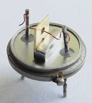
Going deeper, we can look inside the transistor. The board uses type 034 germanium alloy-junction transistors (details, details), very different from modern silicon-based planar transistors. These transistors consist of a germanium crystal base with indium beads fused on either side to form the emitter and collector. The regions of germanium-indium alloy form the "P" regions. In the photo, the germanium disk is in the small circular hole. Copper wires are connected to the indium beads. The photo below shows an IBM 083 transistor from the IBM 1401. This is the NPN version of the transistors in the 3JMX card. If you want a deeper understanding, look at bipolar junction transistor theory, which in turn is explained by quantum physics and solid-state device theory.
[13] You may wonder how 8=4+4 gets computed, since the card described doesn't handle that. The sum 4+4 is computed by the card just below the asterisk (a triple AND gate card of type JGVW). The other two AND gates in that card compute 6+6 and 8+8. To determine what each board in the IBM 1401 does, look at the Automated Logic Diagrams, page 34.32.14.2.
[14] The qui-binary carry logic happens in several phases. The qui parts are added, generating a carry if needed. The binary parts are added with a simple binary adder (not shown). A carry from the binary part shifts the qui part by 2. A carry out signal is also generated as needed. For instance, adding 3 + 5 is done by adding Q2 B1 + Q4 B1. This generates Q6 + B0 + B carry. The B carry increments the qui component to Q8, yielding the result Q8 B0 (i.e. 8).
The qui-binary to BCD translation circuit uses straightforward AND-OR logic, detecting the various combinations. Note that 0 is represented in the 1401 as binary 1010 (because binary 0000 indicates a blank), so the BCD output bits 8 and 2 are set for qui-binary value Q0 B0. The parity output is generate by combining the binary parity (even for B0; odd for B1) with the qui parity value. The qui even parity signal is set for Q0 or Q6, while the qui odd parity signal is set for Q2, Q4, Q8. Note that representing 0 as binary 1010 instead of 0000 doesn't affect the parity.
The error detection circuit uses AND-OR logic to detect bad qui-binary results. It detects a fault if no B bits are set or both B bits are set. Instead of testing every qui bit combination, it implements a short cut from the qui parity circuit. If the even qui parity signal and the odd qui parity signal are both set, this indicates multiple qui lines are set, triggering a fault. If neither qui parity signal is set, then no qui lines are set, also triggering a fault. The parity check misses a few qui combinations (such as Q0 and Q6 set), so these are tested separately. The result is that any invalid qui-binary result triggers a fault.
[15] The rack of cards shown is officially known as gate 01B3. The functions assigned to each card in the photo are approximate, because some cards are used by multiple functions. For exact information, see the plug list, which specifies the card type and function for every card in the 1401.
[16] One complication with the 1401's arithmetic instructions are numbers are stored as a positive value with a sign bit (on the last digit). This format makes printing of positive and negative numbers simpler, which is important for a business computer, but it makes arithmetic more complicated. First, the signs must be checked to determine if the numbers are being added or subtracted. Next, each digit is added or subtracted in sequence until the end of the number is reached. If the result is negative, the 1401 flips the result sign and converts the answer back to a positive value by making two additional digit-by-digit passes over the number. Modern computers use binary and handle negative numbers with two's complement, which makes subtraction much simpler. It takes 9 pages of documentation to explain the addition operation, complete with multiple flowcharts: see IBM 1401 Data Flow pages 24-32. (Keep in mind that these flowcharts are implemented in hardware, not with microcode or subroutines.)
[17] Arithmetic on the 1401 and the qui-binary adder are discussed in detail in 1401 Instruction Logic, pages 49-67. For the history leading up to qui-binary arithmetic, see this article by Carl Claunch.
Ken, is the BCD parity bit used in the conversion to qui-binary? I don't see it as an input. My real question is are there are particular errors they are worried about, i.e. something especially tricky about the addition circuitry? Or just errors in general because this whole computer is a mass of wires and cards? If an error occurs in the addition are there circuits to help you debug the problem?
ReplyDeleteGood stuff as always. I never knew the origin of "mainframe", now I do.
Surely this must be worth a mention or link in the wiki article on 1401?
ReplyDeleteAny page with 17 footnotes must be good!
ReplyDeleteI didn't know about the qui-binary arith, and the 1401 was the second computer I programmed, back when. I love tracing details down to actual transistors on particular cards!
This does tempt me to spend even more time on computer history in the "computer architecture and organization" course I occasionally teach, though; I should probably displace something else if I add much from here.