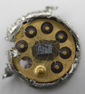
I started with a 741 op amp that was packaged in a metal can (above). Cutting the top off with a hacksaw reveals the tiny silicon die (below), connected to the pins by fine wires.
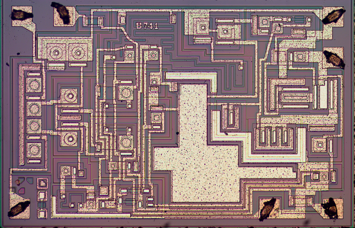
Under a microscope, the details of the silicon chip are visible, as shown below. At first, the chip looks like an incomprehensible maze, but this article will show how transistors, resistors and capacitors are formed on the chip, and explain how they combine to make the op amp.
Why op amps are important
Op amps are a key component in analog circuits. An op amp takes two input voltages, subtracts them, multiplies the difference by a huge value (100,000 or more), and outputs the result as a voltage. If you've studied analog circuits, op amps will be familiar to you, but otherwise this may seem like a bizarre and pointless device. How often do you need to subtract two voltages? And why amplify by such a huge factor: will a 1 volt input result in lightning shooting from the op amp? The answer is feedback: by using a feedback signal, the output becomes a sensible value and the high amplification makes the circuit performance stable.Op amps are used as amplifiers, filters, integrators, differentiators, and many other circuits.[2] Op amps are all around you: your computer's power supply uses op amps for regulation. Your cell phone uses op amps for filtering and amplifying audio signals, camera signals, and the broadcast cell signal.
The structure of the integrated circuit
NPN transistors inside the IC
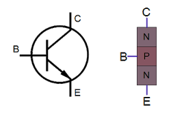
Transistors are the key components in a chip. If you've studied electronics, you've probably seen a diagram of a NPN transistor like the one below, showing the collector (C), base (B), and emitter (E) of the transistor, The transistor is illustrated as a sandwich of P silicon in between two symmetric layers of N silicon; the N-P-N layers make a NPN transistor. It turns out that transistors on a chip look nothing like this, and the base often isn't even in the middle!
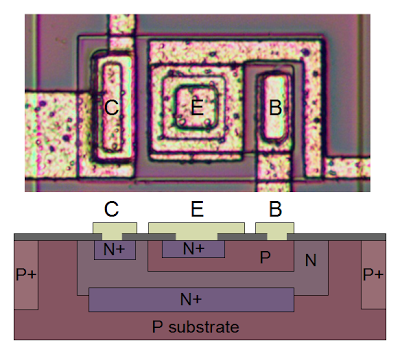
The photo below shows one of the transistors in the 741 as it appears on the chip. The different brown and purple colors are regions of silicon that has been doped differently, forming N and P regions. The whitish-yellow areas are the metal layer of the chip on top of the silicon - these form the wires connecting to the collector, emitter, and base.
Underneath the photo is a cross-section drawing showing approximately how the transistor is constructed. There's a lot more than just the N-P-N sandwich you see in books, but if you look carefully at the vertical cross section below the 'E', you can find the N-P-N that forms the transistor. The emitter (E) wire is connected to N+ silicon. Below that is a P layer connected to the base contact (B). And below that is a N+ layer connected (indirectly) to the collector (C).[3] The transistor is surrounded by a P+ ring that isolates it from neighboring components.
PNP transistors inside the IC
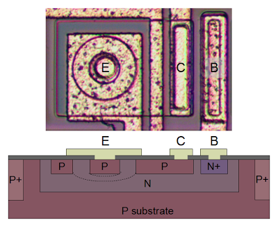
You might expect PNP transistors to be similar to NPN transistors, just swapping the roles of N and P silicon. But for a variety of reasons, PNP transistors have an entirely different construction. They consist of a circular emitter (P), surrounded by a ring shaped base (N), which is surrounded by the collector (P).[4] This forms a P-N-P sandwich horizontally (laterally), unlike the vertical structure of the NPN transistors.The diagram below shows one of the PNP transistors in the 741, along with a cross-section showing the silicon structure. Note that although the metal contact for the base is on the edge of the transistor, it is electrically connected through the N and N+ regions to its active ring in between the collector and emitter.
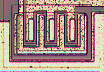
The output transistors in the 741 are larger than the other transistors and have a different structure in order to produce the high-current output. The output transistors must support 25mA, compared to microamps for the internal transistors. The photo below shows one of the output transistors. Note the multiple interlocking "fingers" of the emitter and base, surrounded by the large collector.
How resistors are implemented in silicon
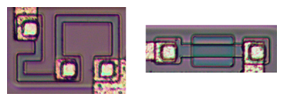
Resistors are a key component of analog chips. Unfortunately, resistors in ICs are very inaccurate; the resistances can vary by 50% from chip to chip. Thus, analog ICs are designed so only the ratio of resistors matters, not the absolute values, since the ratios remain nearly constant from chip to chip.The photo below shows two resistors in the 741 op amp, formed using different techniques. The resistor on the left is formed from a meandering strip of P silicon, and is about 5KΩ. The resistor on the right is a pinch resistor and is about 50KΩ. In the pinch resistor, a layer of N silicon on top makes the conductive region much thinner (i.e. pinches it). This allows a much higher resistance for a given size. Both resistors are at the same scale below, but the pinch resistor has ten times the resistance. The tradeoff is the pinch resistor is much less accurate.
How capacitors are implemented in silicon
The 741's capacitor is essentially a large metal plate separated from the silicon by an insulating layer. The main drawback of capacitors on ICs is they are physically very large. The 25pF capacitor in the 741 has a very small value but takes up a large fraction of the chip's area.[5][6] You can see the capacitor in the middle of the die photo; it is the largest structure on the chip.
IC component: The current mirror
There are some subcircuits that are very common in analog ICs, but may seem mysterious at first. Before explaining the 741's circuit, I'll first give a brief overview of the current mirror and differential pair circuits.
If you've looked at analog IC block diagrams, you may have seen the above symbols for a current source and wondered what a current source is and why you'd use one. The idea of a current source is you start with one known current and then you can "clone" multiple copies of the current with a simple transistor circuit.
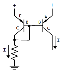
The following circuit shows how a current mirror is implemented.[7] A reference current passes through the transistor on the left. (In this case, the current is set by the resistor.) Since both transistors have the same emitter voltage and base voltage, they source the same current,[8] so the current on the right matches the reference current on the left.
A common use of a current mirror is to replace resistors. As explained earlier, resistors inside ICs are both inconveniently large and inaccurate. It saves space to use a current mirror instead of a resistor whenever possible. [9]
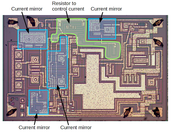
The diagram below shows that much of the 741 die is taken up by multiple current mirrors. The large resistor snaking around the upper middle of the IC controls the initial current. This current is then duplicated by multiple current mirrors, providing controlled currents to various parts of the chip. Using one large resistor and current mirrors is more compact and more accurate than using multiple large resistors. The current mirror in the middle is slightly different; it provides an active load for the input stage, improving the performance.
IC component: The differential pair
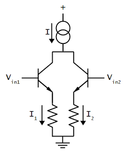
The second important circuit to understand is the differential pair, the most common two-transistor subcircuit used in analog ICs.[10] You may have wondered how the op amp subtracts two voltages; it's not obvious how to make a subtraction circuit. This is the job of the differential pair.
The schematic above shows a simple differential pair. The key is the current source at the top provides a fixed current I, which is split between the two input transistors. If the input voltages are equal, the current will be split equally into the two branches (I1 and I2). If one of the input voltages is a bit higher than the other, the corresponding transistor will conduct more current, so one branch gets more current and the other branch gets less. As one input continues to increase, more current gets pulled into that branch. Thus, the differential pair is a surprisingly simple circuit that routes current based on the difference in input voltages.
The internal blocks of the 741
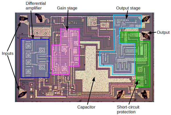
The internal circuitry of the 741 op amp has been explained in many places[11], so I'll just give a brief description of the main blocks. The interactive chip viewer below provides more explanation.The two input pins are connected to the differential amplifier, which is based on the differential pair described above. The output from the differential amplifier goes to the second (gain) stage, which provides additional amplification of the signal. Finally, the output stage has large transistors to generate the high-current output, which is fed to the output pin.
Another feature that made the 741 popular is its short-circuit protection. Many integrated circuits will overheat and self-destruct if you accidentally short circuit an output. The 741, though, includes clever circuits to shut down the output before damage occurs.
Interactive chip viewer
The die photo and schematic below are interactive. Click components in the die photo or schematic[15] to explore the chip, and a description will be displayed below. NPN transistors are highlighted in blue and PNP transistors are in red.
How I photographed the 741 die
Integrated circuit usually come in a black epoxy package. Dangerous concentrated acid is required to dissolve the epoxy package and see the die. But some ICs, such as the 741, are available in metal cans which can be easily opened with a hacksaw.[16] I used this safer approach. With even a basic middle-school microscope, you can get a good view of the die at low magnification but for the die photos, I used a metallurgical microscope, which shines light from above through the lens. A normal microscope shines light from below, which works well for transparent cells but not so well for opaque ICs. A metallurgical microscope is the secret to getting clear photos at higher magnification, since the die is brightly illuminated.[17]Conclusion
Despite being almost 50 years old, the 741 op amp illustrates a lot of interesting features of analog integrated circuits. Next time you're listening to music, talking on your cell phone, or even just using your computer, think about the tiny op amps that make it possible and the 741 that's behind it all.
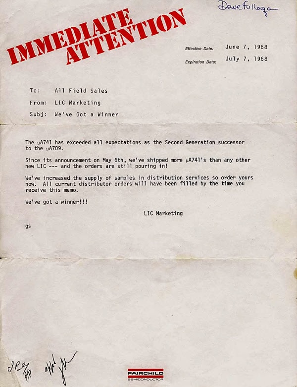
Thanks to Dave Fullagar for providing information on the 741, including the letter above, which shows that the 741 was an instant success.
Notes and references
[1] The 741 op amp is one 25 Microchips That Shook the World and is popular enough to be on mugs and multiple tshirts, as well as available in a giant kit.
[2] To see the variety of circuits that can be built from an op amp, see this op amp circuit collection.
[3] You might have wondered why there is a distinction between the collector and emitter of a transistor, when the simple picture of a transistor is totally symmetrical. Both connect to an N layer, so why does it matter? As you can see from the die photo, the collector and emitter are very different in a real transistor. In addition to the very large size difference, the silicon doping is different. The result is a transistor will have poor gain if the collector and emitter are swapped.
[4] In many of the ICs that I've examined, it's easy to distinguish NPN and PNP transistors by their shape: NPN transistors are rectangular, while PNP transistors have circular emitters and bases with a circular metal layer on top. For some reason, this 741 chip uses rectangular and circular transistors for both NPN and PNP transistors. Thus, a closer examination is necessary to separate the NPN and PNP transistors.
[5] The capacitor in the 741 is located at a special point in the circuit where the effect of the capacitance is amplified due to something called the Miller effect. This allows the capacitor in the 741 to be much smaller than it would be otherwise. Given how much of the 741 die is used for the capacitor already, taking advantage of the Miller effect is very important.
[6] An alternative way to put capacitors on a chip is the junction capacitor, which is basically a large reverse-biased diode junction. The 741 doesn't use this technique; for more information on junction capacitors see my article on the TL431.
[7] For more information about current mirrors, you can check wikipedia, any analog IC book, or chapter 3 of Designing Analog Chips. If you're interested in how analog chips work, I strongly recommend you take a look at Designing Analog Chips.
[8] The current mirror doesn't provide exactly the same current for a variety of reasons. For instance, the base current is small but not zero. Transistor matching is very important: if the transistors are not identical, the currents will be different. (Using a single transistor with two collectors helps with matching.) If the collector voltages are different, the Early effect will cause the currents to be different. More complex current mirror circuits can reduce these problems.
[9] The 741 uses are several common extensions of the current source. First, by adding additional output transistors, you can create multiple copies of the current. Second, if you use a transistor with twice the collector size, you will get an output with twice the current (for instance). Third, instead of multiple output transistors, you can use one transistor with multiple collectors; this seems bizarre if you are used to discrete 3-pin transistors, but is a normal thing to do in IC designs. Finally, by flipping the circuit and using NPN transistors in place of PNP transistors, you can create a current sink, which is the same except current flows into the circuit instead of out of the circuit.
[10] Differential pairs are also called long-tailed pairs. According to Analysis and Design of Analog Integrated Circuits differential pairs are "perhaps the most widely used two-transistor subcircuits in monolithic analog circuits." (p214) For more information about differential pairs, see wikipedia, any analog IC book, or chapter 4 of Designing Analog Chips.
[11] You might expect 741 chips to all be pretty much the same, but the "741" name is really a category, not a single design. Manufacturers use diverse circuits for their 741 chips. Studying data sheet schematics, I found that 741 chips can be be divided into two categories based on the circuits for the second stage and output stage. The more common variant has 24 transistors, while the less common variant has 20 transistors. As far as I can tell, nobody has pointed this out before.
Wikipedia explains the 20-transistor variant while the 24-transistor variants are discussed in Operational Amplifiers IC Op-Amps Through the Ages, UNCC class notes and the book Microelectronic Circuits chapter 12. The 741 die I discuss in this article is the 24-transistor variant.
[12] For details on the 741's history, see this interesting discussion: Computer history museum: Fairchild Oral History Panel.
[13] If the output is too low, the feedback circuit pushes it higher. But if it goes too high, the feedback circuit pulls it lower. This could repeat, causing larger and larger oscillations. The capacitor blocks these oscillations. I've vastly oversimplified op amp stability and frequency compensation. Some more detailed discussions are here and here.
[14] IC Op-Amps Through the Ages says: "Despite a consequent near guarantee of suboptimal performance for most applications [because of the fixed capacitor], the ease of using the 741 has made it tremendously popular, proving Fullager's assumption that engineers are basically lazy (I mean, very time-efficient)."
[15] The schematic is from the Fairchild LM741 datasheet. I added the missing collector-base connection on Q12 and removed R12 (which is unused in this die). The component I photographed is the Analog Devices AD741, but that datasheet doesn't have a schematic.
[16] A plain hacksaw works to cut open an IC can. For later ICs, I used a jeweler's saw which gives a cleaner cut than a hacksaw - the IC doesn't look like it was ripped open by a bear. I got a saw on eBay for $14, and used the #2 blade. Make sure you cut near the top of the IC so you don't hit the internal pins or the die.
[17] To form the large image of the 741 die, I used Microsoft ICE to composite four images into a larger image. The Hugin photo stitcher can also be used for this, but I had trouble with it.
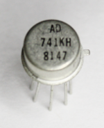

The date code on the 741 looks like its the 47th week of 1981 (8147).
ReplyDeleteNice post! The 25 microchips article estimates that 741s sold in the hundreds of millions - I might have guessed even higher.
ReplyDeleteAn interesting thing about resistors on planar semiconductors: the resistance depends on the aspect ratio of the rectangle (or snake) so resistances tend to be sized in 'squares' - often the exact sheet resistance in ohms per square isn't important. But you do have to account for corners, if you can't match the number of corners. I think a corner is worth about half a square. And orientation might matter too, so try to match that.
In classical (not deep submicron) processes a corner is worth 0.55 of a square IIRC
DeleteThanks for the great writeup the interactive parts are awesome!
ReplyDeleteVery good post and awesome blog !
ReplyDeleteCool post. Thanks!
ReplyDeleteGreat post! When I was a teen (back in the 60's :-) ), I cut open several T0-5 cased transistors and op-amps and this is a GREAT explanation of how circuits are fabricated in silicon. After opening the transistor cases and seeing how tiny the actual die was, it makes perfect sense that tiny circuits could be made from these. I'm bookmarking THIS blog!
ReplyDeletePossibly the best lab experiment I did as an EE undergraduate was to view a 741 under an electron microscope, as I recall as SEM but with the beam switched off. It was fed with a low frequency (0.1Hz maybe) sine wave and was in open loop. So you could see the input stages gradually getting lighter and darker as the charge on them accumulated and dissipated, while the output stages would flip back and forth between light and dark as they were saturating. I think it's the only time I have seen visual evidence that electronics really works at a physical level.
ReplyDeleteGreat post - I really found it interesting. Thanks!
ReplyDeleteBeautiful explanation with beautiful interactive media! I love it
ReplyDeleteBeautiful explanation with beautiful interactive media! I love it
ReplyDeleteTerrific!Learn a lot !
ReplyDeleteMost of the photo links in this post broke when Picasaweb closed. If you get a chance to revisit it, it'd be nice to update them - tiny electronic parts warrant a closer look.
ReplyDeleteJ. Peterson: thanks for letting me know about the links. With considerable effort I've moved all the images off Picasaweb to Amazon S3, which hopefully will be more reliable and won't break my links.
ReplyDeleteGreat article!
ReplyDeleteDo you have a high resolution die image?
It took me a minute to recognize how the capacitors work. Presumably they consist of two large plates, one on top of the other, separated by a dielectric. I would be interested to see a cross-sectional view... would both plates be metal, or would they be made of semiconductor?
ReplyDeleteEvan: the capacitors consist of a metal layer over the silicon, separated by silicon dioxide. The metal forms one plate and the silicon forms the second plate.
ReplyDeleteHave you measured the values of each transistor, such as VCEo, VCBo, VEBo, and hFE?
ReplyDeleteI put those reversed AD741 circuit in spice and it works partially. I found that Q17 emitter 50K ohm resistor seems too big to pull collector of Q7 to low state. I changed this resistor to 50 ohmn. And it works.
ReplyDeleteThis is absolutely awesome!
ReplyDelete