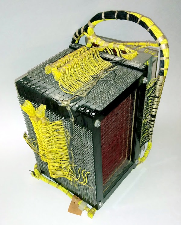
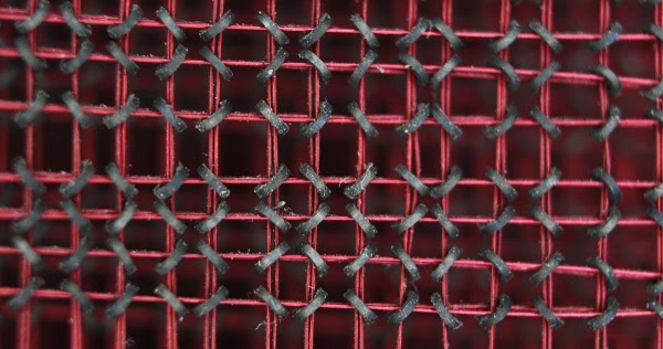
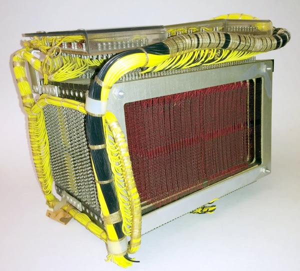
The core module is surprisingly complex, as can be seen above, with thousands of tiny cores mounted on red wires. The module consists of 16 frames stacked together and requires a large amount of wiring. The remainder of the article will dive into the details of this core module. (For an overview of the 1401, see my articles about Bitcoin mining and fractals on the 1401.)
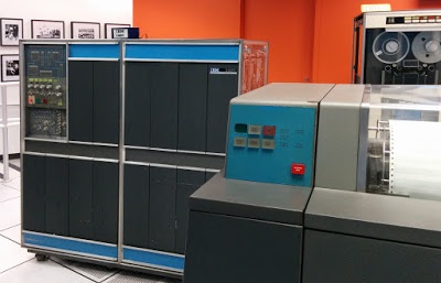
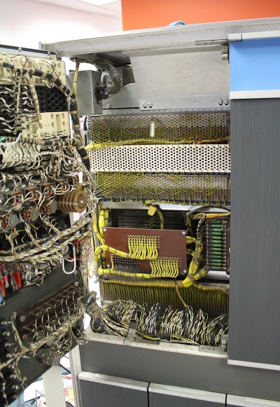
The IBM 1401 mainframe (above) is about the size of two refrigerators. The core memory module in the 1401 can be accessed by swinging open the computer's front panel, as seen below. The console switches, lights, and wiring are on the left. The core module itself is in the center, mostly hidden behind the brown circuit board.
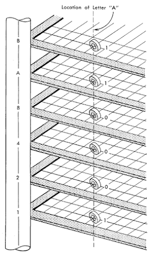
The diagram below illustrates how the character 'A' is stored in core memory. Each bit of data in memory is stored in a tiny ferrite ring or core. These cores can be magnetized in one of two directions, corresponding to a 0 or 1 bit. The cores are arranged into a grid of 4000 cores, called a plane. To select an address, an X wire and a Y wire are activated, selecting the cores where those two wires cross. Each plane stores one bit and planes are stacked up to store a character. You might expect 8 planes are used to store a byte, but the IBM 1401 predates bytes; it uses 6-bit characters based on BCD (binary-coded decimal). Each location also has a special metadata bit called the "word mark", indicating the start of a field or instruction. Adding the parity bit yields eight bits of storage at each address.
Because the IBM 1401 was a business computer, it uses decimal arithmetic rather than binary arithmetic; each character is a binary-coded decimal value, along with two extra "zone bits" for alphanumeric characters.
Since the 1401 uses three-character addresses, you might expect that it could only access 1000 locations.
The trick is the two zone bits of the hundreds character provided the thousands digit 0 to 3.
A consequence is that addresses above 1000 turn into alphanumerics instead of digits; location 2345 is addressed as L45.
Properties of ferrite cores
The physical properties of ferrite cores are critical to the operation of the core memory, so it is important to understand them. First, if a wire through a core carries a strong current, the core will be magnetized according to the direction of the current (following the right-hand rule). Current in one direction will write a 1 to the core, while the opposite current will cause the opposite magnetization and write a 0 to the core.Hysteresis is a key property of the cores: current must exceed a threshold to affect a core's magnetization. A small current will have no effect on the core, but a current above a threshold will cause the core to "snap" into the magnetized state aligned with the current.
The hysteresis property makes it possible to select a particular core. A "half-write" current is sent through the appropriate X select wire and a "half-write" current through the Y select wire. The single core with the selected X and Y wires will have enough current to change state, but the other cores will not have enough current, and will remain unchanged.
The final important property is that when a core switches its direction of magnetization, it induces a current in a sense wire through the core (kind of like a transformer). If the core already has the target state and doesn't change magnetization, no current is induced. This induced current is used to read the state of a core. A consequence is that reading a core erases it, and the desired value must be written back to the core.
Structure of a core plane
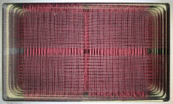
Each core plane has 4000 cores arranged as a 50x80 grid of cores. (The I/O planes are configured differently, and will be explained later.) To reduce interference, the ferrite cores are arranged in a "checkerboard" pattern with each core arranged diagonally in the opposite direction from its neighbors. Four wires pass through each core. The horizontal wires are the X select line and the inhibit line (used for writing). The vertical wires are the Y select line and the sense line (used for reading). The X and Y select lines go through all the planes, so all planes are accessed in parallel.To read a core, the X and Y select lines magnetize the selected cores to the "0" direction. If the core was previously in the "1" state, the core's state change induces a current in the sense wire. If the core was already in the "0" state, no current is induced. Thus, the sense wire allows the bit stored in the core to be determined. The read process destroys the previous value of the core, leaving it in the 0 state. Each plane has a sense wire threaded through all the cores in the plane.
To write a core, current of the opposite polarity is sent through the X and Y select lines to magnetize the core into the 1 state. To keep the core in the 0 state, a current is sent through the plane's inhibit line. The inhibit wire runs through all the cores in a plane parallel to the X select lines. By running the reverse current through the inhibit wire, the X line's current is canceled out, and the core remains unchanged. The inhibit current is too low to flip a core by itself, so other cores are not zeroed out.
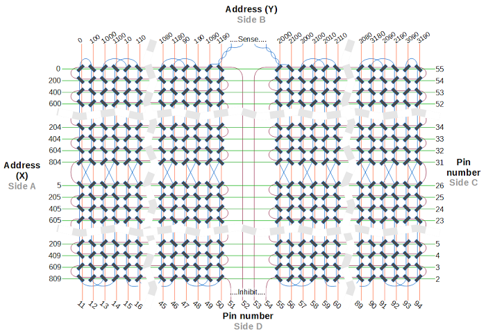
The diagram below shows the reverse-engineered wiring topology of an IBM 1401 core memory plane. Most of the core has been cut out of the diagram, as indicated by the dotted gray lines. The sides of the plane are labeled A through D, matching the 1401 documentation. The A and C sides have 56 pins, while the B and D sides of the plane have 104 pins. Not all the pins are connected.
The X select lines are in green and the Y select lines are in red. The select lines are generated in a complex way by matrix switches, so core addresses are not arranged sequentially. Each matrix switch takes two sets of input lines and activates an output line based on the input values. The 5x10 X matrix switch has 5 row inputs and 10 column inputs, producing 50 outputs, which are the X select lines. The 10 column inputs come from the units digit, and the 5 row inputs are the "even hundreds" digit. The 8x10 Y matrix switch has 8 row inputs and 10 column inputs, producing 80 outputs for the Y select lines. The 10 column inputs are from the tens digit and the 8 row inputs are a tricky combination of the thousands and "odd hundreds". This scheme may seem overly complicated, but it minimizes the hardware required for address decoding.
Each half of the core plane (0-1999 and 2000-3999) has a separate sense line loop, but they are usually wired together. The two sense lines are in blue and run in the Y direction. The sense lines are carefully arranged to avoid picking up interference. The lines cross over along the midpoint to cancel out noise from the Y select lines - the sense line runs in the opposite direction along half of each Y select line, so any induced signal will be canceled out. In addition, the sense lines are twisted as they exit the middle of the plane, to avoid picking up interference. (Many other core memory systems avoid interference by running the sense line diagonally, but the 1401 uses a rectangular layout.)
Each half of the plane has a separate inhibit line. The two inhibit lines are in brown and run next to the X select lines, which they inhibit. The two lines are normally driven separately to reduce noise, but have the same signal. Since the inhibit line switches direction each row, alternating X select lines are also driven in opposite directions.
The card reader/punch, the printer, and the I/O cores
One unusual feature of the core module is the eight special-purpose I/O frames: six core planes and two terminal frames. To understand the I/O cores, some background on the IBM 1401 is necessary. The 1401 was used in business applications such as accounting and payroll, so accuracy was extremely important. If a malfunction caused bad payroll checks to be printed, it would be a catastrophe. To catch problems, IBM put many types of validity checking into the 1401, making it much more reliable than competitors. The basic I/O devices for the 1401 were the card reader/punch and the line printer, separate units from the computer itself and the I/O cores detected problems with these devices.The I/O planes are addressed exactly the same as the data planes. However, the I/O planes are very sparse, with only 297 cores rather than 4000 cores, so most locations have no storage as can be seen in the photo below. These planes are accessed by the I/O circuitry, and are invisible to the programmer.
The IBM 1401 uses 80-character punch cards. You might expect the card reader to read each character on the card in sequence and send the character to the computer, but that's not at all how it works. Instead, the card reader processes each card "sideways" for speed, using 80 metal brushes to read a row at a time. If a card has a hole in a position, the brush contacts a metal roller under the card, completing a circuit. The brushes are connected to the IBM 1401 by 80 wires, one for each brush. Each wire is connected directly to a "row-bit core" in the core memory module, setting the core if a hole was detected. There's no driver circuitry or memory addressing; it's literally a separate wire from each brush that is wrapped 5 times around a core. Let me emphasize how unusual this is: it's like having a separate wire from each key on your keyboard directly to a specific transistor in your memory chip.
The card reader/punch has three read stations: RD1 and RD2 for reading, and PCH for reading after punching. Since each read station has 80 brushes, 240 wires connect the brushes to the 240 row-bit cores. (As you might have guessed, the cables between the 1401 computer and the reader/punch are very thick.) As well as the row-bit cores, reading/punching uses core planes called XU, YU, XL, and YL to count the number of holes detected in each position. If the two read stations have different hole counts, the computer stops and reports a fault. Likewise, the count is checked after punching a card to make sure all holes were punched correctly.
The high-speed line printer uses 132 hammers to produce 132-column output. A chain with the 48 printable characters whizzes around horizontally. As each character on the chain passes a position where it should be printed, a hammer fires at the precise time, hitting the paper against the inked ribbon to print the character. The I/O cores are also used to detect problems in the printing process.
Printing uses several different core planes for multiple validity checks. Each of the 132 print hammers is wired directly to a "hammer-fire core" in the memory module. The XU core plane is used during printing for the print-compare check: a bit is set in the XU plane if a hammer should fire for the character position. These 132 bits are compared with the hammer-fire cores to verify that the correct hammers fired. Plane YL holds print-line complete cores that verify that every character position either printed a character or holds a non-printable character. Finally, to aid printer maintenance, plane YU records the location of any fault in print-error storage core.
Physical layout of the core module
The core module consists of 16 frames in a stack - 14 core planes and two terminal frames. The upper 8 frames hold the character data planes and the lower 8 frames are the I/O frames. The following table shows the usage of each frame. The terminal frames do not contain cores, but provide connections for the large wire bundles from the reader brushes and the print hammers.
| 1: | Bit 8 |
| 2: | Bit 4 |
| 3: | Bit 2 |
| 4: | Bit 1 |
| 5: | Bit A |
| 6: | Bit B |
| 7: | Parity |
| 8: | Word Mark |
| 9: | Terminals for frame 10 |
| 10: | Card reader brushes (RD2), punch brushes (PCH) |
| 11: | Terminals for frame 12 |
| 12: | Card reader brushes (RD1), print hammers (PRT) |
| 13: | XU (I/O) |
| 14: | YU (I/O) |
| 15: | XL (I/O) |
| 16: | YL (I/O) |
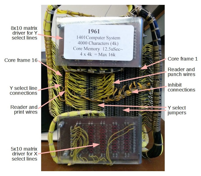
The picture below shows the large amount of wiring required by the core module. Frame 16 (YL) is at the left and frame 1 (bit 8) is at the right. The two matrix switches are on the front of the module: the 8x10 switch for the Y select lines is at top, and the 5x10 switch for the X select lines is at the bottom.
The yellow wires at the left and right connect the Y select lines on frame 16 and frame 1 to the 8x10 matrix switch. Two bundles of wires connect to I/O planes near the middle of the module. One connects the brushes in the card reader and the printer hammer drivers to terminals on frame 11. The other bundle connects read brushes and punch check brushes to terminals on frame 9. The horizontal wire bundle across the middle of the planes connects the inhibit lines of each plane.
The photo below provides another view, focusing on the data plane wiring. At front is frame 1, the core plane for data bit 8, with the gray cores visible on red wires. The other 15 frames are layered behind frame 1. The two matrix switches are on top. The 8x10 matrix switch is connected to the Y select lines on the top and the 5x10 matrix switch is connected to the X select lines on the left.
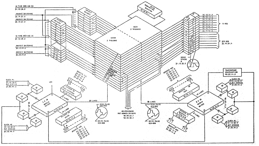
The detailed block diagram below shows how the components are connected in the 1401's core memory system. This diagram shows the physical arrangement of the 16 frames in the core memory module, along with the driver circuitry. The inhibit drivers are at the upper left, feeding each core plane. The sense amplifiers are at the upper right. The 5x10 X matrix switch is in the lower left, and the 8x10 Y matrix switch is in the lower right. Note the read brushes, punch brushes, and print hammer drivers are wired directly into the core module through the terminal frames. The diagram also shows the timing of the read and write pulses, and how they have opposite polarity, writing 0 and 1 respectively.
The matrix switches
Generating the X and Y select signals is a tricky problem. The drive signals must have a positive pulse of the right current and duration for reading, followed by a negative pulse for writing. In addition, the number of select lines is large (50 X and 80 Y), so hardware costs would be excessive if each line had its own driver circuitry.The 1401 uses an interesting solution to drive the select signals. Matrix switches generate the select signals by using a set of ferrite cores. But instead of storage, these cores are used for their switching properties. As with storage, the matrix switch depends on the "coincident current" property, where two signals of sufficient current will cause a core to snap to the opposite magnetization. But instead of being used for storage, the cores in the matrix switch generate a drive signal.
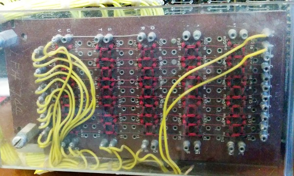
The photo above shows the X matrix switch. The switch consists of 50 cores in a 5 by 10 grid, with 5 lines driving the rows and 10 lines driving the columns. Each core also has an output winding and a bias winding. When two input lines are triggered, the corresponding core flips state, generating a pulse on the output winding. When the input lines are released, the bias winding flips the core back to its original state, generating a negative pulse on the output winding. Thus, the desired one of the 50 outputs has a positive pulse followed by a negative pulse, which is just what the core module requires for read followed by write.
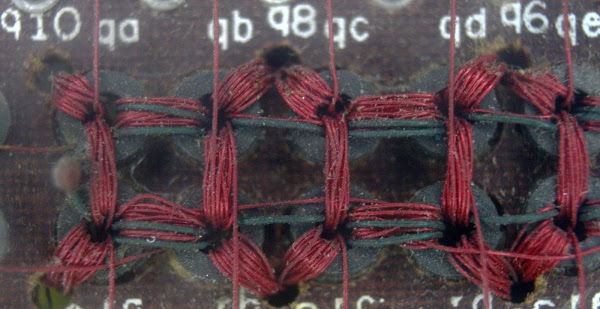
The photo below shows the wiring of the matrix switch cores. The bias wire (black) is wound through pairs of cores three times. Each horizontal input wire (red) is wound through pairs of cores about twelve times, as are the vertical input wires. Each core has an output wire wound diagonally about twelve times.
How core memory is mounted in the 1401
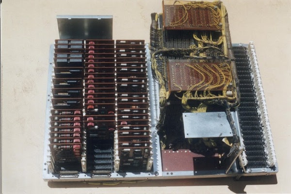
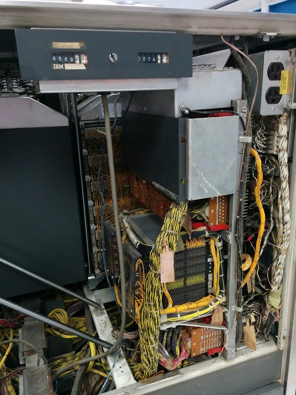
The following picture shows the core memory module mounted in its rack, along with the many SMS cards required by the core module. (IBM built computers from Standard Modular System cards, each about the size of a playing card and holding a few transistors and other components.) At the left are the driver cards and current source cards that drive the matrix switch boards, and the driver cards for the inhibit lines. The next column holds the address decode cards. The address lines plug into the empty sockets at the bottom. The next column holds the sense line pre-amplifier and amplifier cards. The core module itself is mounted with the matrix switch cards on top. At the far right are the sockets for the hundreds of wires from the brushes and print hammers.The photo below shows the core module mounted inside the IBM 1401 mainframe, looking into the left end of the computer. The core module is behind the bundle of black and yellow wires, mostly address lines. The matrix switches are on the left. The colorful brush and hammer wires are connected via paddles underneath the core module. The SMS driver cards are above the core module, mostly behind a metal cover for airflow.
The photo shows some other interesting features of the 1401. At the top of the computer is the time meter that records how much time the computer has been running. IBM usually leased the 1401 and if you used the computer more than 8 hours per day, they would charge you for the excess. (Unless, of course, you paid for the 24/7 lease.) In the upper right is the "convenience" outlet located inside the computer, a standard electrical outlet. Below the outlet is the wiring on the back of the front console. The computer didn't use a backplane; instead, many loose bundles of wires connected circuitry modules, as you can see at the bottom of the photo.
Conclusion
Core memory was the leading memory technology from the mid-1950s until it was replaced by semiconductor memory in the early 1970s. For its time, core memory provided dense, reliable, and inexpensive storage, but memory technology has improved incredibly since then. The 1401 had a 11.5 microsecond memory cycle time, compared to 5 nanoseconds for modern RAM. While the 1401 had 4000 characters of storage (expandable to 16K), modern computers have many gigabytes. Adding a 4K memory expansion to the 1401 cost $20,100 ($162,000 in current dollars). Now a 16 gigabyte memory costs under $100. But even though it is obsolete, core memory is still an interesting technology to examine.Thanks to the members of the 1401 restoration team and the Computer History Museum for their assistance The IBM 1401 is demonstrated at the Computer History Museum on Wednesdays and Saturdays (subject to hardware problems) so check it out if you're in Silicon Valley (schedule).

6 comments:
My father worked for IBM during the years of these machines.
So I an interested in the first place.
But these old machines just so fascinating, and your writing is so intricate and in-depth, I would love it anyway.
Consider me a fan.
BT
Ken, your hot link for "address decode cards" points to the AQV Z Driver card instead of the AQU "Alloy Switch, Decoder Number 2" card.
If you are short on spares for 091, 086, and 071, I have researched modern substitutes. (The Bob Hunter list is wrong.)
Dave Wise in Hillsboro Oregon
Keeper of the Last Running 1620
I remember the 1401 well as I programed and operated it. The 1st one we initially installed had only 4k of memory. I now carry a smart phone that has a memory size 6.5 million times larger.
I have what I think may be an historic core matrix switch of Russian origin but to date no one can identify its function, 10inch x 10inch board, huge cores. Can send images if anyone can help.
I happen to have some pieces of this core memory. Some are completely intact while others have broken plastic. These are, at least to me, important as I used an IBM 1401 when I was in college many years ago.
I worked on a 1401 at Merritt College in Oakland. We also had a 141 simulator (abbreviated 1401) that ran on an IBM 1620. Some years later I was wandering through an electronics surplus store at the old Oakland Airport and found a single 1401 core plane (along with bunches of those lighted push-button switches from various old IBM systems-including a 1620). Still have that core plane on my bookshelf.
Post a Comment