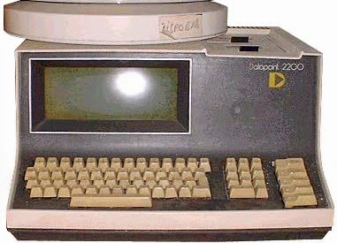
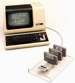
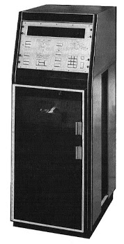
The story starts with the Datapoint 2200[1], a "programmable terminal" sized to fit on a desktop. While originally sold as a terminal, the Datapoint 2200 was really a minicomputer that could be programmed in BASIC or PL/B. Some people consider the Datapoint 2200 the first personal computer as it came out years before systems such as the Apple II or even the Altair.
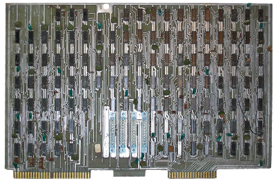
The Datapoint 2200 had an 8-bit processor built out of dozens of TTL chips, which was the normal way of building computers at the time. The photo below shows the processor board. Keep in mind that there's no processor chip—the whole board is the processor, with a chip or two for each register, a few chips for the adder, a few chips to decode instructions, a few chips to increment the program counter, and so forth. [28] Nowadays, we think of MOS chips as high-performance and building a CPU out of TTL chips seems slow and backwards. However, in 1970, TTL logic was much faster than MOS. Even operating one bit at a time as a serial computer, the Datapoint 2200 performed considerably faster than the 8008 chip, unless it needed to wait for the slow serial memory.
While building the Datapoint 2200, its designers were looking for ways to make the processor board smaller and generate less heat. Datapoint met with Intel in December 1969, and what happened next depends on whether you listen to Intel or Datapoint. Intel's story is that Datapoint asked if Intel could build memory chips for the processor stack that had an integrated stack pointer register. Intel engineer Stan Mazor told Datapoint that Intel could not only do that, but could put the whole 2200 processor board on a chip.[2][3] Datapoint's story is that Datapoint founder Gus Roche and designer Jack Frassanito suggested to Intel's co-founder Robert Noyce that Intel build a single-chip CPU with Datapoint's design.[4] but Noyce initially rejected the idea, thinking that a CPU chip wouldn't have a significant market.
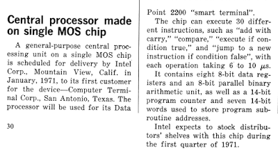
In any case, Intel ended up agreeing to build a CPU chip for Datapoint using the architecture of the Datapoint 2200.[5] Intel developed a functional specification for the chip by June 1970 and then put the project on hold for six months. During this time, there was a mention of future 8008 chip in Electronic Design (below)—I suspect I've found the first public mention of the 8008. You might expect there was a race to build the first microprocessor, so you may be surprised that both the 4004 and 8008 projects were put on hold for months. Meanwhile, Datapoint built a switching power supply for the 2200[6], which eliminated the heating concerns, and was planning to start producing the 2200 with the processor board of TTL chips. Thus, Datapoint wasn't particularly interested in the 8008 any more.
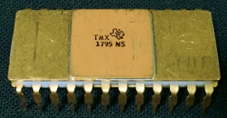
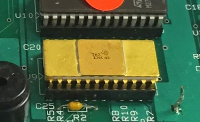
A Texas Instruments salesman learned that Intel was building a processor for Datapoint and asked if Texas Instruments could build them one too. Datapoint gave TI the specifications and told them to go ahead. Texas Instruments came up with a three-chip design, but came up with a single-chip CPU after Datapoint pointedly asked, "Can't you build it on one chip like Intel?" Texas Instruments started building a CPU for Datapoint around April 1970 and this chip became the TMX 1795.
There's a lot of debate on just how much information about Intel's design was given to Texas Instruments. The main TI engineer on the project, Gary Boone, says they received hints that Intel was doing better, but didn't improperly receive any proprietary information. According to Intel, though, Texas Instruments received Intel's detailed design documents through Datapoint. For instance, the TI processor copied an error that was in Intel's documentation leaving the TI chip with broken interrupt handling.[7]
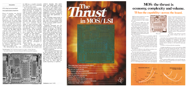
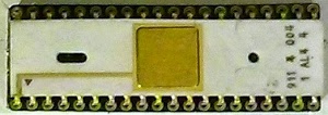
The TI chip was first mentioned in March, 1971 in Businessweek magazine, in a short paragraph calling the chip a "milestone in LSI [Large-Scale Integration]" for jamming the CPU onto a single chip.[8] A few months later, the chip received a big media launch with an article and multi-page advertising spread in Electronics (below), complete with die photos of the TMX 1795.
The article, entitled "CPU chip turns terminal into stand-alone machine", described how the chip would make the Datapoint 2200 computer much more powerful. "The 212-by-224 mil chip turns the 2200 into a complete computer that doesn't have to be connected to a time-sharing system." The components of the chip are "similar to units previously available separately, but this is the first time that they've been combined monolithically", consolidated "into a single chip". The chip and 2K of memory would cost about $100. This "central processor on a chip" would make the new Datapoint 2200 "a powerful computer with features the original one couldn't offer."
That didn't happen. Datapoint tested the TMX 1795 chip and rejected it for four reasons. First, the chip and memory didn't tolerate voltage fluctuations of more than 50mV. Second, the TMX 1795 required a lot of support chips (although not as many as the 8008 would), reducing the benefit of a single-chip CPU. Third, Datapoint had solved the heat problem with a switching power supply.[6] Finally, Datapoint had just about completed the 2200 Version II, with a much faster parallel implementation of the CPU. The TMX 1795 (operating in parallel) was slightly faster than the original serial Datapoint 2200, but the 2200 Version II was much faster than the TMX 1795. (This illustrates the speed advantage of TTL chips over MOS at the time.)
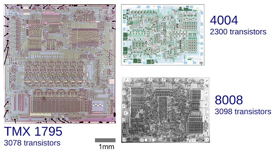
Intel engineers provided another reason for the commercial failure of the TMX 1795: the chip was too big to manufacture cost-effectively. I created the diagram below to compare the TMX 1795, 4004, and 8008 at the same scale. The TMX 1795 is larger than the 4004 and 8008 combined! One reason is that Intel had silicon-gate technology, which in effect allowed three layers of circuitry instead of two. But even taking that into account, Texas Instruments didn't seem to put much effort into the layout, which Mazor calls "pretty sloppy techniques" and "throwing some blocks together".[9] While the 4004 and especially the 8008 are densely packed, the TMX 1795 chip has copious unused and wasted space.
As well as rejecting the TMX 1795, Datapoint also decided not to use the 8008 and gave up their exclusive rights to the chip. Intel, of course, commercialized the 8008, announcing it in April 1972. Two years later, Intel released the 8080, a microprocessor based on the 8008 but with many improvements. (Some people claim that the 8080 incorporates improvements suggested by Datapoint, but a close examination shows that later Datapoint architectures and the 8080 went in totally different directions.) The 8080 was followed by the x86 architecture, which was designed to extend the 8080. Thus, if you're using an x86 computer now, you're using a computer based on the Datapoint 2200 architecture.[10]
Some sources dismiss the TMX 1795 as a chip that never really worked. However, the video below shows Gary Boone demonstrating the TMX 1795 in 1996. A TMX 1795 board was installed in a laptop (probably a TI LT286) for the purpose of the demo. It runs a simple text editor, a sort program, a simple budget spreadsheet, and Fibonacci numbers. The demo isn't particularly thrilling, but it shows that the TMX 1795 was a functional chip.
Considering the size of Intel and the microprocessor market, Datapoint's decision to give up exclusive rights to the 8008 seems like a huge blunder, possibly "one of the worst business decisions in history". However, it's unlikely that Datapoint would have sold 8008 chips, given that they were a computer company, not a chip company like Intel.[11] In addition, Intel had plans to produce microprocessors even without the rights to the 4004 or 8008.[12]
After rejecting the TMX 1795 (and the 8008), Datapoint continued to build processors out of TTL chips until the early 1980s. While these processors were faster and more powerful than microprocessors for a surprisingly long time, eventually Moore's law led to processors such as the 80286, which outperformed Datapoint at a lower cost. Under heavy competition from PCs, Datapoint's stock crashed in 1982, followed by a hostile takeover in 1984. The company limped along before going bankrupt in 2000. Given that Datapoint designed the architecture used in the 8008, it's ironic that Datapoint was killed by x86 microprocessors which were direct descendents of the 8008.
Unlike Intel, who commercialized the 8008 chip, Texas Instruments abandoned the TMX 1795 after Datapoint's rejection. The chip would have disappeared without a trace, except for one thing, which had a huge impact on the computer industry.
The "Dallas Legal Firm" and "TI v. Everybody"[13]
Texas Instruments figured out early on that patent litigation and licensing fees could be very profitable. After (co-)inventing the integrated circuit and receiving patents on it, Texas Instruments engaged in bitter patent battles, earning the nickname "the Dallas legal firm" for their "unethical and unprofessional legal tactics".[13] Texas Instruments continued their legal practices with the TMX 1795, receiving multiple patents on it, issued between 1973 and 1985.[14][15]Needless to say, Intel was not happy that Texas Instruments patented the TMX 1795, since building a single-chip processor for Datapoint was Intel's idea.[16] Intel was even unhappier that that Texas Instruments had used parts of Intel's specification when designing and patenting the TMX 1795.[7][17] Intel had wanted to patent the 4004[18], but their patent attorney told them that it wasn't worth it, and the idea of putting a computer on a chip was fairly obvious. Likewise, Datapoint had considered patenting the single-chip microprocessor but was told by their patent attorney that there was nothing patentable in the idea.[3]
In order to extract substantial licensing fees, Texas Instruments sued multiple companies using their microprocessor and microcontroller patents (including the TMX 1795 patent) in a case that Gordon Bell called "TI v. Everybody".[13] Dell decided to fight back in a "bet the company" lawsuit.[14] The lawsuit dragged on for years and was about to go to trial when the case suddenly turned against Texas Instruments.
Lee Boysel of Four-Phase Systems had built a 24-bit MOS-based minicomputer in 1970, as will be discussed in more detail below. The computer had a 9-chip CPU, but in an amazing hack, Boysel took one of the three 8-bit arithmetic/logic chips and was able to build a working microcomputer from it. Since this chip was a year before than the TMX 1795, it torpedoed Texas Instruments' case and it never went to trial. As a result, many people consider the Four-Phase AL1 to be the first microprocessor. However, as I'll explain below, the demo wasn't quite what most people think.
Is the TMX 1795 really the first microprocessor?
There's a fair bit of argument of what is the first microprocessor. Several candidates for first microprocessor were introduced in a short period of time between 1968 and 1971. These are all interesting chips, but most of them have been forgotten. In this section, I'll discuss various candidates, but first I'll look at whether it makes sense to consider the microprocessor an invention.Giving some hardware background will help the following discussion. The transistors you're probably most familiar with are bipolar transistors—they are fast, but bipolar integrated circuits can't contain large numbers of transistors. The TTL chips used in the Datapoint 2200 and other systems are built from bipolar transistors. A later technology produced MOS transistors, which are slower than bipolar, but can now be squeezed onto a chip by the millions or billions. The final term is LSI or Large-Scale Integration, referring to an integrated circuit containing a large number of components: 100 gates or more. The introduction of MOS/LSI is what made it possible to build a processor with a few chips or a single chip, rather than a board full of chips.
The inevitability of microprocessors
One perspective is that the microprocessor isn't really an invention, but rather something that everyone knew would happen, and it was just a matter of waiting for the technology and market to be correct. This view is convincingly presented in Schaller's thesis,[19] which has some interesting quotes:The idea of putting the computer on a chip was a fairly obvious thing to do. People had been talking about it in the literature for some time.—Ted Hoff, 4004 designer
At the time in the early 1970s, late 1960s, the industry was ripe for the invention of the microprocessor.- Hal Feeney, 8008 designer
The question of ‘who invented the microprocessor?’ is, in fact, a meaningless one in any non-legal sense. - Microprocessor Report
I largely agree with this perspective. It was obvious in the late 1960s that a CPU would eventually be put on a chip, and it was just a matter of time for the density of MOS chips to improve to the point that it was practical. In addition, in the 1960s, MOS chips were slow, expensive, and unreliable[11]—a computer built out of a bunch of bipolar chips was obviously better, and this included everything from the IBM 360 mainframe to the PDP-11 minicomputer to the desktop Datapoint 2200. At first a MOS-based computer only made sense for a low-performance application (calculators, terminal), or when high density was required (aerospace, calculators).
To summarize this view, the microprocessor wasn't anything to specifically invent, but just something that happened when MOS technology improvements and a marketing need made it worthwhile to build a single chip processor.
Defining "microprocessor"
Picking the first microprocessor is largely a linguistic exercise in how you define "microprocessor". It also depends on how you define "first": this could be first design, first manufactured chips, first sales, or first patent. But I think for reasonable definitions, the TMX 1795 is first.There's no official definition of a microprocessor. Various sources define a microprocessor as a CPU on a chip, or an arithmetic-logic unit (ALU) on a chip, or on a few chips. One interesting perspective is that "microprocessor" is basically a marketing term driven by the need of companies like Intel and Texas Instruments to give a label to their new products.[11]
In any case, I consider a microprocessor to be a CPU on a single chip, including the ALU, control, and registers. Storage and I/O is generally outside the chip. There will generally be additional support and interface chips such as buffers, latches, and clock generation. I also consider it important that a microprocessor be programmable as a general-purpose computer. This definition, I think, is a reasonable definition for a microprocessor.
One architecture that I don't consider a microprocessor is a microcoded system, where the control unit is separate and provides micro-instructions to control the ALU and the rest of the system. In this system, the microcode can be provided by a ROM and a latch steps through the micro-instructions. Since the ALU doesn't need to do instruction decoding, it can be a much simpler chip than a full-blown CPU. I don't think it's fair to call it a microprocessor.
Timeline of early microprocessors
There are several processors that are frequently argued to be the first microprocessor, and they were created in a span of just a few years. I created the timeline below to show when they were developed. In the remainder of this article, I describe the different processors in detail.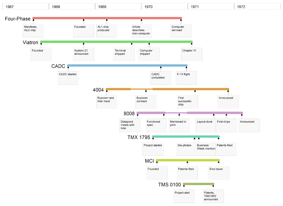
Four-Phase AL1
If one person could be considered the father of MOS/LSI processors, it would be Lee Boysel. While working at Fairchild, he came up with the idea of a MOS-based computer and methodically designed and built the necessary cutting-edge chips (ROM in 1966, ALU in 1967, DRAM in 1968). Along the way he published several influential articles on MOS chips, as well as a 1967 "manifesto" explaining how a computer comparable to the IBM 360 could be built from MOS.
Boysel left Fairchild and started Four-Phase Systems in October 1968 to build his MOS-based system. In 1970, he demoed the System/IV, a powerful 24-bit computer. The processor used 9 MOS chips: three 8-bit AL1 arithmetic / logic chips, three microcode ROMs, and three RL random logic chips. This computer sold very well and Four-Phase became a Fortune 1000 company before being acquired by Motorola in 1981.
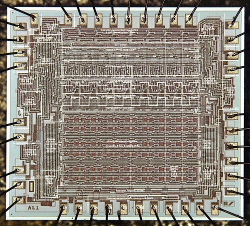
As described earlier, Boysel used an AL1 chip as a processor in a courtroom demonstration system in 1995 to show prior art against TI's patents. Given this demonstration, why don't I consider the AL1 to be the first microprocessor? It used an AL1 chip as the processor, along with ROM, RAM, and I/O and some address latches, so it seems like a single-chip CPU. But I've investigated this demonstration system closely, and while it was a brilliant hack, there's also some trickery. The ROM and its associated latch are actually set up as a microcode controller, providing 24 control lines to the rest of the system. The ROM controls memory read/write, selects an ALU operation, and provides the address of the next microcode instruction (there's no program counter). After close examination, it's clear that the AL1 chip is acting as an Arithmetic/Logic chip (thus the AL1 name), and not as a CPU.
There are a few other things that show the AL1 wasn't working as a single-chip computer. The die photo published as part of the trial has the components of the AL1 chip labeled, including "Instruction Register 23 bits". However, that label is entirely fictional—if you study the die photo closely, there's no instruction register or 23 bits there, just vias where the ground lines pass under the clock lines. I can only conclude that this label was intended to trick people at the trial. In addition, the AL1 block diagram used at the trial has a few subtle changes from the originally-published diagram, removing the program counter and adding various interconnections. I examined the code (microcode) used for the trial, and it consists of super-bizarre microcode instructions nothing like the AL1's original instruction set.
While the demo was brilliant and wildly successful at derailing the Texas Instruments lawsuits, I don't see it as showing the AL1 was a single-chip microprocessor. It showed that combined with a microcode controller, the AL1 could be used as a barely-functioning processor. In addition, you could probably use a similar approach to build a processor out of an earlier ALU chip such as the 74181 or Fairchild 3800, and nobody is arguing that those are microprocessors.
Looking at the dates, it appears that Viatron (described below) shipped their MOS/LSI computer a bit before Four-Phase, so I can't call Four-Phase the first MOS/LSI computer. However, Four-Phase did produce the first computer with semiconductor memory (instead of magnetic core memory), and thus the first all-semiconductor computer.
Viatron
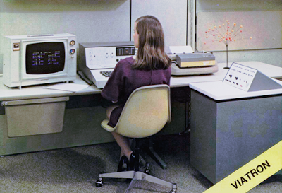
Viatron is another interesting but mostly forgotten company. It began as a hugely-publicized startup founded in November, 1967. About a year later, they announced System 21, a 16-bit minicomputer with smart terminals, tape drives, and a printer, built from custom MOS chips. The plan was volume: by building a large number of systems, they hoped to produce the chips inexpensively and lease the systems at amazingly low prices—computer rental for $99 a month.[20] Unfortunately, Viatron ran into poor chip yields, delays, and price increases. As a result, the company went spectacularly bankrupt in March 1971.
Viatron is literally the originator of the microprocessor—they were the first to use the word "microprocessor" in their October 1968 announcement of the 2101 microprocessor. However, this microprocessor wasn't a chip—it was an entire smart terminal, leasing for the incredibly low price of $20 a month. Viatron used the term microprocessor to describe the whole desktop unit complete with keyboard and tape drives. Inside the microprocessor cabinet were a bunch of boards—the processor itself consisted of 18 custom MOS chips on 3 boards, with more boards of custom MOS and CMOS chips for the keyboard interface, tape drive, memory, and video display.
The 3-board processor inside the 2101 was specialized for its terminal role. It read and wrote multiple I/O control lines, moved data between I/O devices and memory, updated the display, and provided serial input and output.[20] The processor was very limited, not even providing arithmetic. Nonetheless, I think the Viatron 2101 "microprocessor" can be considered the first (multichip) MOS/LSI processor, shipping before the Four Phase System/IV.
Viatron also built an advanced general-purpose 16-bit computer, the 62-pound 2140 minicomputer, which leased for $99 a month and came with a Fortran compiler. It had 4K 16-bit words of core memory and two 16-bit arithmetic units. The microcoded processor had an extensive instruction set including multiply and divide operations, and supported 48-bit arithmetic. Coming on the market slightly before the Four-Phase computer, the Viatron 2140 appears to be the first MOS/LSI general-purpose computer. Unfortunately, sales were poor and the 2140 projected ended in 1973.
MP944 / F-14 CADC
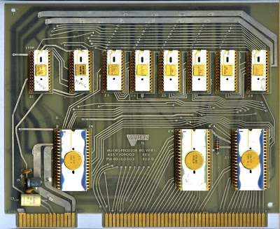
The Central Air Data Computer was a flight control system for the F-14 fighter, using the MP944 MOS/LSI chipset developed between 1968 and 1970. This computer processed information from sensors and generated outputs for instrumentation and to control the aircraft. The main operation it performed was computing polynomial functions on the inputs. This chipset was designed by Ray Holt, who argues on his website (firstmicroprocessor.com) that this 20-bit serial computer should be considered the first microprocessor.
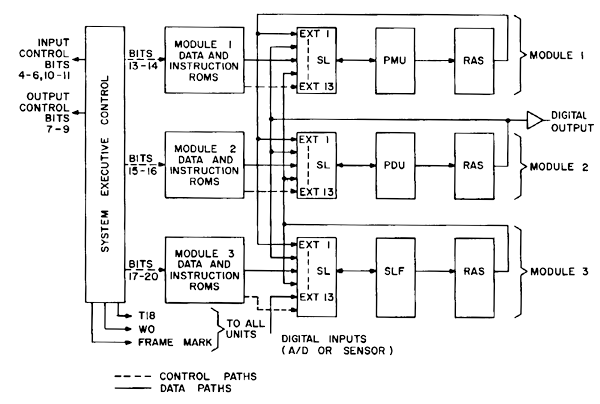
The architecture of this computer is pretty unusual; it consists of three functional modules: a multiplier, a divider, and "special logic". Each functional unit has a microcode ROM (including an address register) that provides a 20-bit microinstruction, a data steering unit (SL) that selects between 13 data inputs and performs addition, the arithmetic chip (multiply (PMU), divide (PDU) or special logic (SLF)), and a small RAM chip for storage (RAS). Each data line transfers a 20-bit fixed-point value, shifted serially one bit at a time. The main purpose of the SLF (special logic function) chip is to clamp a value between upper and lower bounds. It also converts Gray code to binary[21] and performs other logic functions.[22]
I don't consider this a microprocessor since the control, arithmetic, and storage are split across four separate chips in each functional unit.[23] Not only is there no CPU chip, there's not even a general-purpose ALU chip. Computer architecture expert David Patterson says, "No way Holt's computer is a microprocessor, using the word as we mean it today."[24] Even if you define a microprocessor as including a multi-chip processor, Viatron beat the CADC by a few months. While the CADC processor is very interesting, I don't see any way that it can be considered the first microprocessor.
Intel 4004
The well-known Intel 4004 is commonly considered the first microprocessor, but I believe the TMX 1795 beat it. I won't go into details of how Busicom contracted with Intel to have the 4004 built for a calculator, since the story is well-known.[25] I did a lot of research into the dates of the 4004 to determine which was first: the 4004 or the TMX 1795. According to the 4004 oral history, the first successful 4004 chip was the end of February 1971 and shipped to Busicom in March. TI wrote a draft announcement with photos of the TMX 1795 on February 24, 1971, and it was written up in Businessweek in March. The TMX 1795 was delivered to Datapoint in the summer and TI applied for a patent on August 31. The 4004 wasn't announced until November 15.To summarize, the dates are very close but it appears that the TMX 1795 chip was built first (assuming the chip was working for the Feb 24 writeup) and announced first, while the 4004 was delivered to customers first. On the other hand, Federico Faggin claims that the 4004 was a month or two before the TMX 1795[17]. However, the TMX 1795 was patented; I assume that someone would have mentioned in all the patent litigation if the 4004 really beat the TMX 1795 (rather than building a demo out of the Four-Phase AL1). Based on the evidence, I conclude that the TMX 1795 was slightly before the 4004 as the first microprocessor built, while the 4004 is clearly the first microprocessor sold commercially. Texas Instruments claims on their website: "1971: Single-chip microprocessor invented", and I agree with this claim.
Intel 8008
Many people think of the Intel 8008 as the successor to the 4004, but the two chips are almost entirely independent and were developed roughly in parallel. In fact, some of the engineers on the 4004 worried that the 8008 would come out first because the 8008 project consisted of one chip to the four in the 4004 project. The 8008 was originally called the 1201 in Intel's naming scheme because it was the first custom MOS chip Intel was developing. The 4004 would have been the 1202 except Faggin, a key engineer on the project, convinced management that 4004 was a much better name. The 1201 was renamed the 8008 before release to fit the new naming pattern.According to my research, the 8008 may be the first microprocessor described in print. I found a reference to it (although without the 8008 name) in a four-paragraph article in Electronic Design in Oct 25, 1970, discussing Intel's chip under development for the Datapoint 2200. The article briefly describes the chip's instruction set, architecture, and performance. It said the processor would be used in the 2200 "smart terminal" (which of course didn't happen), and said the chip was scheduled for January, 1971 delivery (it slipped and was officially announced in March 1972).
Gilbert Hyatt's microcontroller patent
The story of how Gilbert Hyatt obtained a broad patent covering the microcontroller in 1990 and lost it a few years later is complex, but I will try to summarize it here. The story starts with the founding of Micro-Computer Incorporated in 1968. Hyatt built a 16-bit serial computer out of TTL chips and sold it as a numerical control computer. He had plans to build this processor as a single chip, but before that could happen, the company went out of business in 1971. Mr. Hyatt claims that investors Noyce and Moore (of Intel fame) cut off funding because "their motive was to sell the company and take the technology."
In 1990, seemingly out of nowhere, Gilbert Hyatt received a very general patent (4942516) covering a computer with ROM and storage on a single chip. Hyatt had filed a patent on his computer in 1969, and due to multiple continuations, he didn't receive the patent until 1990.[15] This patent caused considerable turmoil in the computer industry since pretty much every microcontroller was covered by this patent. Hyatt ended up receiving substantial licensing fees until Texas Instruments challenged the patent a few years later and the patent office canceled Hyatt's key patent claims.[26] In any case, Gilbert Hyatt's microprocessor was never built (except in TTL form), there was no design for it, and the patent didn't provide any information on how to put the computer on a chip. Thus, while this computer built from TTL chips is interesting, it never became a microprocessor.
TMS 0100 calculator-on-a-chip / microcontroller
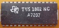
Texas Instruments created the TMS 1802NC calculator-on-a-chip in 1971; this was the first chip in the TMS 0100 series.[27] This chip included program ROM, storage, control logic and an ALU that performed arithmetic on 11-digit decimal numbers under the control of 11-bit opcodes.
While the TMS 0100 series was usually called a calculator-on-a-chip, it was also intended for microcontroller tasks. The patent describes "Programming of the calculator system for non-calculator functions", including digital volt meter, tax-fare meter, scale, cash register operations, a controller, arithmetic teaching unit, clock, and other applications. As the first "computer-on-a-chip", the TMS 0100 gave Texas Instruments several important microcontroller patents. which they used in patent litigation (including the Dell case described earlier).[14] (The key difference between a microcontroller and a microprocessor is the microcontroller includes the storage and program ROM, while the microprocessor has them externally.)
The TMX 1795 (first microprocessor) and TMS 0100 (first microcontroller) were both developed by Gary Boone and team (Mike Cochran, Jerry Vandierendonck, and others) at Texas Instruments almost simultaneously, which is a remarkable accomplishment. The TMS1802NC / TMS 0100 was announced September 17, 1971.
In 1974, Texas Instruments released the successor to the TMS 0100 series, the TMS 1000 series, and marketed it as a microcontroller. Externally, the TMS 1000 series had I/O similar to the TMS 0100 series, but internally it was entirely different. The 11-bit opcodes of the TMS 0100 were replaced by 8-bit opcodes and the 11-digit decimal storage was replaced by 4-bit binary storage. Some sources call the TMS 1000 series the first microcontroller or first microprocessor. This is entirely wrong and based on confusion between the two series. Confusing the TMS 0100 and TMS 1000 is like confusing the 8008 and 8080: the latter is a related, but entirely new chip.
Conclusions
Because the TMX 1795 wasn't commercially successful, the chip is almost forgotten, even though the chip has an important historical role. I've uncovered some history about this chip and take a detailed technical look at other chips that are sometimes considered the first microprocessor. The "first microprocessor" title depends on how exactly you define a microprocessor, but the TMX 1795 is first under a reasonable definition—a CPU-on-a-chip. It's interesting, though, how multiple MOS/LSI processor chips were built in a very short span once technology permitted, and how most of them are now almost entirely forgotten. In a future article, I'll look at the implementation and circuitry of the TMX 1795 in detail.Thanks to Austin Roche for detailed information on Datapoint. Thanks to K. Kroslowitz of the Computer History Museum" for obtaining TMX 1795 photos for me; the chip is so obscure, there were no photos of it on the internet up until now.
Notes and references
[1] The Datapoint Corporation was founded in 1968 as CTC (Computer Terminal Corporation), CTC later changed its name to Datapoint as the name of its product was much better known than the company name itself. For simplicity, I'll use Datapoint instead of CTC to refer to the company in this article.[2] The Computer History Museum's Oral History Panel on the Development and Promotion of the Intel 8008 Microprocessor discusses the history of the 8008 in great detail. The story of the initial idea to build a single chip for Datapoint is on page 2. Texas Instruments' chip development is on page 3-4. The use of little-endian format is discussed on page 5. TI's chip is discussed on page 6. Automated design of TI's chip is on page 25.
[3] The Computer History Museum's Oral History of Victor (Vic) Poor provides a lot of history of Datapoint. Page 34 describes Stan Mazor suggesting that Intel put Datapoint's processor on a single chip. Page 43 describes the TI chip and its noise issues. Page 46 explains how Datapoint's patent attorney told them there was nothing patentable about the single-chip microprocessor.
[4] Much of the information on Datapoint comes from the book Datapoint: The Lost Story of the Texans Who Invented the Personal Computer Revolution. The story of Datapoint suggesting a single-chip CPU to Noyce is on pages 70-72.
[5] The 8008 processor was originally given the number 1201 under Intel's numbering scheme. The first digit indicated the type of circuitry: 1 for p-MOS. The second digit indicated the type of chip: 2 for random logic. The last two digits were a serial number. For some reason, the 4004 was numbered after the 8008 and would have been the 1202. Fortunately, its developers argued that 4004 would be a better name for marketing reasons. The 1201 was later renamed the 8008 to fit this pattern. Thus, the 8008 is often though of as a successor to the 4004, even though the chips were developed in parallel and have totally different architectures.
[6] A switching power supply is much more efficient than the less complex linear power supplies commonly used at the time, so it generates much less heat. The Datapoint 2200 used a push-pull topology switching power supply. Steve Jobs called the Apple II's power supply "revolutionary", saying "Every computer now uses switching power supplies, and they all rip off Rod Holt's design." Note that the Datapoint 2200 with its swiching power supply came out 6 years before the Apple II. I've written a lot more about the history of switching power supplies here. (By the way, don't confuse Ray Holt of the CADC with Rod Holt of Apple.)
[7] According to Ted Hoff[18], Intel had a flaw in the original interrupt handling specification for the 8008 and TI copied that error in the TMX 1795, demonstrating that TI was using Intel specifications. In particular, when the 8008 processor is interrupted, a RESTART instruction can be forced onto the bus, redirecting execution to the interrupt handler. The stack pointer must be updated by the RESTART instruction to save the return address, but Intel didn't include that in the initial specification. (The RESTART instruction is not part of the original Datapoint architecture.)
I've verified from the patent that the RESTART logic in the TMX 1795 doesn't update the stack pointer, so interrupt handling is broken and there's no way to return from an interrupt. (The interrupt handling section of the TMX 1795 patent is kind of a mess. It discusses a "CONTINUE" instruction that doesn't exist.) According to Ted Hoff, this demonstrates that Texas Instruments was using Intel's proprietary specification without entirely understanding it.
[8]
The text of the TMX 1795 announcement in Businessweek, March 27 1971, p52:
"Computer Terminal Corp., of San Antonio, Tex., has designed a
remote cathode-ray computer terminal no bigger than a typewriter that also
functions as a powerful minicomputer. In what must rank as a milestone in LSI,
Texas Instruments has managed to jam this terminal's entire central processing unit-
the equivalent of 3,100 MOS transistors-on a single custom chip roughly 2 in. square."
[9] In the Intel 8080 Oral History, the layout of the TMX 1795 is criticized on page 35.
[10] One enduring legacy of the Datapoint 2200 is the little-endian storage used by Intel x86 processors, which is backwards compared to most systems. Because the Datapoint 2200 had a serial processor, it accessed bits one at a time. For arithmetic, it needed to start with the lowest bit, in order to handle carries (the same as long addition starts at the right). As a consequence of this, Datapoint 2200 instructions had the low-order byte before the high-order byte. There's no need for a processor accessing bits in parallel to be little endian: processors such as the 6800 and 8051 use the more natural big-endian format. But all the microprocessors descended from the 8008 (8080, Z80, x86) kept the little-endian format used by Datapoint. (See also 8008 Oral History, page 5.)
[11] The perspective that Four-Phase and Intel treated the microprocessor differently because For Phase was a computer manufacturer and Intel is a chip manufacturer is discussed at length in When is a microprocessor not a microprocessor? in Exposing Electronics. This also goes into the history of Boysel and Four-Phase. It contains the interesting remark that the Texas Instruments litigation turned an old integrated circuit (the Four-Phase AL1) into a new microprocessor. Related discussion is in the book To the Digital Age: Research Labs, Start-up Companies, and the Rise of MOS Technology.
[12] While designing the 4004, Intel had a little-known backup plan in case the 4004 turned out to be too complex to build. This backup plan would also allow Intel to sell processors even though Busicom had exclusive rights to the 4004. (The 4004 was built under contract to calculator manufacturer Busicom, who had exclusive rights to the 4004 (which they later gave up). Federico Faggin explains (Oral History) that while Busicom had exclusive rights to use the 4004, they didn't own the intellectual property, so Intel was free to build similar processors.) This backup plan was the simpler 4005 chip. While the 4004 had 16 registers and an on-chip stack, the 4005 just had the program counter, a memory address register, and an accumulator, using external RAM for registers. When the 4004 chip succeeded, Intel didn't need the 4005 and licensed it to a Canadian company, MicroSystems International, which released the chip as the MF7114 in the second half of 1972. Sales were poor and the MF7114 was abandoned in 1973, so the chip is almost unknown today. The history of the MF7114 is described in detail in The MIL MF7114 Microprocessor.
[13] The description "TI versus Everybody trial" is from The Evolution to the Computer History Museum" by Gordon Bell, p28. Texas Instruments was referred to as "The Dallas Legal Firm" by the CEO of Cypress Semiconductors according to History of Semiconductor Engineering p 194-195.
[14] Texas Instruments received several broad patents on the TMX 1795. 3,757,306: "Computing Systems CPU" covers a CPU on a single chip with external memory. 4,503,511: "Computing system with multifunctional arithmetic logic unit in single integrated circuit" covers an ALU, registers, and logic on a chip. 4,225,934: "Multifunctional arithmetic and logic unit in semiconductor integrated circuit" describes an ALU on a single chip with a parallel bus.
The Texas Instruments v. Dell litigation featured multiple patents. The TMX 1795 patent in the litigation was 4,503,511: "Computing system with multifunctional arithmetic logic unit in single integrated circuit"; the other TMX 1795 patents were not part of the litigation. Several were TMS 0100 calculator/microcontroller patents: 4,326,265: "Variable function programmed calculator", 4,471,460: "Variable function programmed system", 4,471,461: "Variable function programmed system", 4,485,455: "Single-chip semiconductor unit and key input for variable function programmed system". Finally there were some miscellaneous patents: 3,720,920: "Open-ended computer with selectable I/O control", 4,175,284: "Multi-mode process control computer with bit processing", RE31,864: "Self-test feature for appliance or electronic systems operated by microprocessor".
The broader lawsuit Texas Instruments v. Daewoo, et al was against computer manufacturers Cordata (formerly Corona Data Systems), Daewoo, and Samsung. It went on from 1990 to 1993, and ended up with the companies needing to license the patents. The Dell lawsuit, Texas Instruments v. Dell, also went from 1990 to 1993 but ended in a settlement favorable to Dell after Boysel's demonstration of the AL1 chip acting as a single-chip CPU in 1992.
[15] It may seem strange that someone can get a patent a decade or two after their invention. This is accomplished through a "continuation", which lets you file updated patents with additional claims. This process can be dragged out for decades, resulting in a submarine patent.
Patents used to be good for 17 years from the date it was granted, no mater how delayed. This delay can make a patent much more valuable; there are a lot more companies to sue over a microprocessor patent in 1985 than in 1971, for instance. Plus, if you have a similar non-delayed patent too, it's like having a free extension on the patent. US patents are now valid for 20 years from filing, eliminating submarine patents (except for those still in the system).
[16] Ted Hoff's article Impact of LSI on future minicomputers, IEEE International Convention Digest, Mar. 1970, discusses the difficulty of building LSI parts that can be used in large (and thus cost-effective) volumes. He suggests that since a MOS chip can hold 1000 to 6000 devices, a standardized CPU could be built on a single LSI chip and sold for $10 to $20.
[17] The 4004 Oral History has information on the 4004 timeline. Federico Faggin says that the TI chip was a month or two after the 4004 (page 32). Page 33 discusses the interrupt problem on the TMX 1795.
[18] Interview with Marcian (Ted) Hoff (archived) provides a lot of background on development of the 4004. It describes how by October 1969 they were committed to building the 4004 as a computer on a chip. The first silicon for the 4004 was in January 1971, and by February 1971 the chip was working. In May 1971, Busicom ran into financial difficulties and negotiated a lower price for the 4004 in exchange for giving up exclusive rights to the chip. He describes how at the Fall Joint Computer Conference, many customers would argue that the 4004 wasn't a computer but just a bit slice; after looking at the datasheet, they realized that it was a computer. Ted Hoff also describes the origins of the 8008, saying that he and Stan Mazur proposed the single-chip processor to Datapoint, much to Vic Poor's surprise, but later Vic Poor claimed that he had planned a single-chip processor all along.
[19] The thesis Technological Innovation in the Semiconductor Industry by Robert R. Schaller, 2004, has several relevant chapters. Chapter 6 analyzes the history of the integrated circuit in detail. Chapter 7, The Invention of the Microprocessor, Revisited, provided a lot of background for this article. Chapter 8 is a detailed analysis of Moore's Law.
[20] By carefully studying the Viatron terminal schematics, I uncovered details about the multi-chip processor in the Viatron terminal. The processor handled 8-bit characters and was programmed in 12-bit microcode, 512 words stored in ROM chips. It had three data registers (IBR, TEMP, and AUX), and two microcode ROM address registers (RAR and RAAR). Arithmetic operations appear to be entirely lacking from the processor. The memory was built from shift register memory chips and was used for the display. The Viatron price list is in the Viatron System 21 Brochure.
[21] The Gray code is a way of encoding values in binary so only one bit changes at a time. This is useful for mechanical encoding because it avoids errors during transitions. For instance, if you use binary to encode the position of an aircraft control, as it moves from 3 to 4 the binary values are 011 and 100. If the first bit changes before the rest, you get 111 (i.e. 7) and your plane may crash. With Gray code, 3 and 4 are encoded as 010 and 110. Since only one bit changes, it doesn't matter if the bits don't change simultaneously—you either have 3 or 4 and no bad values in between.
[22] Ray Holt's firstmicroprocessor.com calls the SLF (special logic function) chip the CPU. In the original paper, this chip was not called the CPU and was only described briefly. In the paper, each of the three multi-chip functional units is called a CPU. It's clear that the SLF chip was recently renamed the CPU just to support the claim that the CADC was the first microprocessor.
[23] The MP944 chips had considerably fewer transistors than the 4004: 1063 in the PMU, 1241 in the PDU, 743 in the SLF, and 771 in the SLU, compared to 2300 in the 4004.
[24] David Patterson's analysis of the CADC computer can be found on the firstmicroprocessor.com website.
[25] The inventors of the 4004 wrote a detailed article about the chip: The history of the 4004. Other articles with details on the 4004's creation are The birth of the microprocessor and The Microprocessor.
[26] For more information on Gilbert Hyatt's patent, see Chip Designer's 20-Year Quest and For Texas Instruments, Some Bragging Rights, Inventor battling U.S. over patents from '70s and Gilbert Who? An obscure inventor's patent may rewrite microprocessor history.
The specific legal issues and maneuvering over Hyatt's patent are complex, but described in the appeal summary and Berkeley Technology Law Journal. If you try to follow this, note that Boone's '541 application and '541 patent are two totally different things, even though they have the same title and end in 541. The presentation Patent litigations that shaped their industries provides an overview of the litigation over the "Single Chip Computer" and other inventions.
[27] Note that the TMS 0100 is actually a series of chips (TMS 01XX) and likewise the TMS 1000 is also a series. Confusingly, the first chip in the TMS 0100 series was the TMS 1802NC calculator chip, which was renamed the TMS 0102; despite its name, it was not in the TMS 1000 series.
[28] The Datapoint 2200 was a serial processor—while it was an 8-bit processor, it operated on one bit at a time, had a one-bit ALU, and a one-bit internal bus. While this seems bizarre from our perspective, implementing a processor serially was a fairly common way to reduce the cost of a processor; the PDP-8/S was another serial minicomputer. (This should not be confused with the Motorola MC14500B, which genuinely is a one-bit processor designed for simple control applications.)

Thanks for a great article. I worked on the Z80 at Mostek, also on their ill-fated version of the 68000. I enjoy the history.
ReplyDeleteA word of caution on the Datapoint book by Lamont Wood: it's basically self-published by one of the former Datapoint people, John Frassanito. Which is not to claim that there's anything wrong with it (I haven't read it myself) but it's surely Frassanito's telling of the story.
ReplyDeleteGood work. Always fun to read anything that credits Datapoint as "at the creation".
ReplyDeletebtw, although you mentioned CMOS CPU speed later in the article, it was, as my Datapoint colleagues of the time (I joined in Jan 71), "main board" designer Gary Asbell (deceased) and assembly language designer/programmer Harry Pyle told me, the overwhelming reason for rejecting the Intel or TI CMOS CPUs was CMOS's much slower clock speed of a few 100 KHz versus their proven "main board" of small and medium scale TTL running MUCH faster. iow, even all the other problems could be solve, the CMOS CPUs speed would always be the show stopper. So SSI/MSI TTL won.
Len Conrad
Is the history of the Hewlett Packard "nanoprocessor" (partno 1820-1691 and ...92) fully unravelled at this point ?
ReplyDeleteSome of the date-codes I have seen can put it very early in the race.
Poul-Henning
Thanks for the great article.
ReplyDeleteWhenever I click an image on the article It shows as 'not found' on Picasa.
Great research and write-up Ken! One quibble with your analysis of little-endian versus big-endian: note that the 6502 gains some cycles of performance advantage over the similar 6800 by having both operands and indirect addresses appear LSB first, because indexing arithmetic is performed byte-serial.
ReplyDeletePoul-Henning: thank you for the interesting note on the HP "nanoprocessor", which I hadn't heard of. There's not much information on it, so let me know if you have a concrete date. One source said that it was NMOS, which would suggest it came after PMOS chips like the 8008. Another source said it was based on the BPC processor, which was in 1972. Another source says the BPC was the first microprocessor HP built. So my guess is the nanoprocessor was 1972 or later.
ReplyDeleteAnonymous: I think I've figured out the Picasaweb permissions and hopefully the photos work now.
Ed: yes, the 6502 gets an advantage from little-endian. On the other hand, the 6800 went big-endian. I guess the difference is the indexed absolute addressing the 6502 has.
Nice write up.
ReplyDeleteIt all comes down to the definition of a microprocessor.
When bringing up a definition one should try to not exclude anything beforehand - after all, we want to do an open ended search, don't we?
While you're right, that such a beast must reside on a single chip (for the major parts), I do not realy count versions with an external micro programm ROM out per se. After all, microcode is just a way to formulate a task with less abstraction - and VLIW systems do go the very same path. It doesn't realy matter for the existance of a computer if a task is formulated in a more abstract way which again is interpreted by microcode or not. Thus ruling out the AL1 as 'too little' isn't as easy as it seams.
Similar the exclusion of systems with more components than the bare minimum may need some rethinking. Just because a TMS1802 already includes ROM and I/O, doesn't make the processor part disapear from the chip. It's much like the first car (Benz three wheeler) already includes a passenger seat, so not only beeing the first motor car, but also the first passenger car.
Last but not least, unusual ways of data processing like serial formats, decimal numbers or specialized streaming structures should not rule out a concept. To be named a processor, a design should be turing complete. No matter how aweful programming might be, as long as it's possible to do anything, it's a computer.
So puting this together, a definition for 'microprocessor' would fit all devices that are capable of running general progamms, where all main components reside on a chip. Programm and data storage may or may not be on chip. Similar for I/O.
Did I miss anything?
Thank you for telling this story again... Tech users of today know NOTHING of how computing works...OR, computers!! Technologists are REAL hard to find.. Especilly someone that knows where all these glittering toys came from.
ReplyDeleteThe company where I had my first real eye-opening into the depth of what computing was about, was a small speciality publishing company near Chicago. We bought, and used with an astounshing result, Datapoint 2200 serial numbers 2 and 6. Over the course of a couple of years, we used the 2200's as input devices for specialty text, and thru other, computer-related programming radically changed the face of the publishing industry.
GREAT place to pinpoint the start of a future...
In that TI Electronics ad, it's amusing to see a figure that looks a lot like Moore's...
ReplyDeleteWasn't the main reason for Datapoint's demise the discovery they were double-accounting for orders not yet manufactured as already delivered?
ReplyDeleteThis comment has been removed by the author.
ReplyDeleteLamont Wood wrote a book, Datapoint: The Lost Story of the Texans Who Invented the Personal Computer Revolution. I'm about halfway through it, and it does a good job of recounting the stories behind the creation of Datapoint and their relationships with TI and Intel.
ReplyDeleteThanks for the great article"
ReplyDeleteFirst, congratulations on an excellent article. Very few people, even among those who pay attention to the history of computers prior to 1975, are aware of all of these chips and systems. Even fewer can recognize their relative significance.
ReplyDeleteI agree with your conclusion that the TMX 1795 was the first operational microprocessor, but have different opinions about several other items. Also, I agree strongly with the position expressed in "The inevitability of microprocessors" -- the single-chip microprocessor was, at best, a minor invention, and inevitable once the major invention of the integrated circuit had been made about a decade earlier. There was a major invention within the set of products you discuss -- the concept of the desktop PC -- achieved by the Datapoint 2200 -- a complete system with CPU, memory, bulk storage, display, keyboard, I/O ports, and an operating system in a single desktop enclosure with a footprint suitable for use on a desk.
First, I contend that the 4004 should be excluded from consideration as the first microprocessor for the same reason as the CADC -- the 4004 was NOT a general-purpose computer. While the block diagram of the 4004 looks like that a conventional CPU, the 4004 had two, physical separate address spaces for program code and data, and the 4004 instruction set provided NO means for writing to program memory (even if said memory were implemented using RAM instead of the 4001 ROM+I/O chips intended as program store for the 4004). Furthermore, program memory space was organized 4Kx8, whereas data memory space was organized 1280x4 (and accessible only 20x4 at a time, so really more of a banked register space than general purpose data memory), hence a major hardware hack would have been needed to provide any manner of write access to program memory. Each of the Four-Phase, Viatron, and Datapoint 2200-derived CPUs used conventional, general-purpose architectures, including a unified, flat, read/write address space.
Second, I disagree with your conclusion that the Four-Phase was the first computer with solid state memory. If the basis for "first” is the date of the article describing the computer, then the first all-solid-state computer is the ILLIAC IV, which was extensively described in articles published in 1969. However, ILLIAC IV was not operational until late 1971 (so ought to be considered to be the first supercomputer with solid state memory). If the basis for "first" is the date of the public demonstration and/or delivery, then the Datapoint 2200, IBM System/7, and Data General SuperNova SC all preceded Four-Phase. Also, the IBM System 370/145, the first mainframe with solid-state memory, was announced in October 1970, although I do not believe it was demonstrated, nor delivered, until well into 1971. At best, the Four-Phase is the first system with both a general-purpose LSI CPU and solid-state memory.
I would like to offer a few clarifications about the 2200 and the relationship between the Datapoint and Intel versions of the architecture. I was an early user of both the 2200 and 8008, and several years later worked as a processor architect at Datapoint, so I was able to cross-check my "external" view of that history with people who were directly involved.
ReplyDeleteThe sole reason the Datapoint 2200 Version I was a serial design was memory cost, and as soon as 1K-bit DRAMs were available in the required quantities the 2200 Version II, with a parallel CPU and double the maximum memory capacity, was introduced. In 1969 the only available form of solid-state memory was dynamic MOS shift registers. These were especially low cost for Datapoint, because they were purchasing large quantities of 512-bit shift registers for use as the refresh memory of their extremely popular Datapoint 3300 glass TTY product. It is worth keeping in mind that, when Datapoint approached Intel about making a custom CPU chip for the 2200, they were Intel's largest customer.
The greater speed of the 2200 Version II, versus the Version I and the 8008, was primarily due to its use of RAM and a parallel data path, not its use of TTL circuitry. Minimum instruction execution time on the Version I was 8 microseconds, but this ballooned to 520 microseconds whenever an operand had to be fetched from or stored into memory because a full “rotation” of the shift registers was required before the next instruction could be fetched. The Version II’s parallel CPU achieved instruction times of 1.6 to 4.8 microseconds and with RAM there was no penalty for non-sequential access. It is also worth noting that the 2200 Version II (and subsequent Datapoint processors) had two sets of CPU registers, switchable using a single instruction -- a feature most people associate with the Z-80, introduced five years later.
While there is no doubt that the architecture of subsequent Datapoint and Intel processors diverged, I would stop short of saying that "later Datapoint architectures and the 8080 went in totally different directions." The divergence began when Datapoint needed 16-bit capabilities long before Intel could put a 16-bit processor on a chip. Datapoint extended the architecture while maintaining full upward compatibility from the 2200. 16-bit operations were implemented using pairs of 8-bit registers rather than widening the registers as on the 8086. The most significant area where Datapoint took a different direction than Intel was by expanding address space beyond 64KB and adding memory protection using paging rather than segmentation. The most important aspects of the programming model -- the CPU registers and condition codes -- remained equivalent all the way through the Datapoint 8000-series processors and the Intel 80286. Two developments at Datapoint illustrate the closeness of the two architectures: In the late 1970s the Datapoint 1500 series used the Z-80. Datapoint's DOS for ran with minimal modification. In the early 1980s, after the failure of a project to develop a single-chip successor to the 6600 CPU (with the consequence that the Datapoint 8600 went to market with a TTL emulator for the failed LSI chip), Datapoint developed a relatively simple hardware block known internally as the “TLX Engine”. The TLX logic sat in front of an 80286 and translated Datapoint instructions to Intel instructions on-the-fly. Had the instruction sets not had a nearly direct mapping, and especially if the condition codes and register side effects not been essentially identical, this would not have been practical. The Datapoint 8400 (1983) and 7600 (1986) were desktop workstations using 6MHz TLX Engines. The Datapoint 7900 (1986) was an SMP server with four 10MHz TLX Engines. The TLX was dropped from the next generation of Datapoint products because the 80386 could emulate the Datapoint instruction set in software at comparable or better speeds.
ReplyDeleteYes, finally confirmation to my doubts about AL1 court presentation. First time when I heard that setup, I was sure that is made by microcode trick.
I have ever seen that good resolution die photo of AL1 and it is now obvious that is not CPU in any means, just part of it.
But how you forgot GI/Pico Electronics calculator chip?
http://www.spingal.plus.com/micro/4001566.pdf
It is also claimed (wrongly) first CPU.
Ps. Nice blog, here is always something interesting to read. Thanks!
Wonderful piece.
ReplyDeletePicked you up from the 1401/Bitcoin article via LCM on Facebook, and it's clear you should be a Regular Read; what is *not* clear is why Datamation or someone isn't *paying you* to write to this quality. :-)
Your How Bitcoin Mining Works article, BTW, is the only one I have ever come across that I could actually understand, though I *still* don't quite get where the "15 coin bonus" for a mined block *comes from*; it seems to be created whole cloth.
Back on this piece: TMS1802 is a name that sounds, as our TVTropes friends would put it, "suspiciously similar" to that of RCA's CDP1802 CMOS CPU, which dates to roughly the same period; any thoughts on that?
Baylink: thanks for your kind words. As for as the TI TMS 1802 and RCA CDP 1802, they are totally different and the RCA chip was 5 years later so it's just a confusing coincidence that they have the same number. RCA had their 1800 series and numbered chips sequentially. Ti probably was numbering sequentially too.
ReplyDeleteSimilarly, RCA introduced the CD4004 binary counter in 1969 as part of the 4000 series. This is, of course, totally unrelated to the 4004 microprocessor.
Some friends bought an early game console, I think it was the RCA Studio II, based on the 1802. They hacked a keyboard into the system, and took advantage of the games video display to create a complete system.
ReplyDeleteOn the same subject, in 1981, a large group of engineers at Mostek reverse engineered the Apple II, including the 80 column card, and included 64K bytes of DRAM in an excellent clone. It costs $300 for a complete box of parts, including chips, caps, resistors, keyboard, power supply, and case. Wish I bought one.
This article fills in the blanks of my own blog that I started writing after I found one the first Datapoint CPU boards with parts on it from 1969 along with Intel's first run of 3101 static memory chips. Datapoint is the world's first microcomputer although calling it a PC is a bit of a reach.
ReplyDeletemfischer: Thank you for your detailed comments. I had similar concerns about whether the 4004 should be considered a general-purpose microprocessor or just a hardcoded controller. However, Intel created the 4008/4009 interface chips which allowed standard RAM to be used as program memory that the 4004 could write to. Thus, the 4004 isn't restricted to just ROM programs. Also, the Intellec MCS-4 is a microcomputer using the 4004 that runs an assembler and can be programmed via a connected terminal. The 4004 is clearly being used as a microprocessor here, even if the address space organization is more Harvard than von Neumann.
ReplyDeleteRegarding the first computer with solid-state memory,
I haven't researched memory history myself, so you may be quite right about the earlier systems.
I used the source "To the Digital Age", p257: IBM claimed the System/370 Model 145 was the first computer with semiconductor main memory, but Four Phase actually beat them.
Have you seen my article on the
Intel 1405 shift register memory chips that Datapoint used?
To clarify my statement that later Datapoint architectures and the 8080 went in totally different directions, I meant that later Datapoint and Intel processors were based on the Datapoint 2200 / 8008 architecture, but the changes from the original architecture were entirely independent in the two companies.
Specifically, Datapoint added two register banks (2200 II); added prefixes for 16-bit instructions, block instructions and an entirely new X register (5500); and added assorted instructions such as linked list support (6600). The 8080 didn't take any of those ideas, but implemented totally different 16-bit (i.e. register pair) instructions and simplified the I/O instructions dramatically.
I've seen claims that Intel's evolution from the 8008 to the 8080 was based on Datapoint's suggestions, but after examining the instruction sets closely, I don't see any influence from Datapoint post-8008.
Finally, mfischer: can you send me an email? I expect to have Datapoint questions for you in the future. (My address is in the sidebar.)
Hi Ken Sherrif,
ReplyDeleteMy email ID is [email protected]
I had a doubt regarding an IC used in a mobile Phone USB charger that i bought recently.
The name of the IC is CSC 7101C AVCcM.
I am not able to find any datasheet for such a name.
I really need to know the internals of the IC.
Really impressed with your work and know that you can definitely solve my issue.
Thanks And Regards,
Bhupesh Gargi
India
Hi Ken, Don't think we have met yet. This is Ray Holt, designer of the CADC mentioned in this article. You did a good job researching some unknown history.
ReplyDeleteI wish to make an initial reply on your comment on my architecture. Having a multiplier and divider in parallel to a CPU is not unusual, just years ahead of the "co-processor" concept.
Re-labeling the SFF to CPU was nothing but a clarification to what it really did. Had nothing to do with 1st, 2nd or 3rd. Silly conclusion without asking me first.
I really find it interesting that very few are technical enough to recognize a 20-bit parallel divider and multiplier (with carry look-ahead) in any architecture is a HUGE accomplishment on the current P-channel technology .... by the way the exact technology used in the Intel 4-bit two years later.
Lastly, for now, it is also interesting that most early designs were concept only, did not work, or only worked in limited situations. The F14 CADC was not only current technology but ran a MIL-SPEC rating and worked perfectly the first time.
I would love to have a conversation on any of the early designs and technology and to put some real comments on architecture, definitions and any other concerns.
Fortunately, some of us are still alive that really know what went on. By the way, I also consulted for Intel in 1973-74 on marketing and training for the 4004 while having to keep secret the CADC for 30 years .... until 1998.
Ray Holt
Hi Ray! Thank you for writing. I've looked at the CADC system in detail and I hope to write more about it at some point, since it's very interesting but not as well known as it should be. I've studied your papers about it and I'd be interested in any additional information you can share. Do you have sample code and more details on the instruction set? Also, high-resolution die photos would be very informative.
ReplyDeleteKen
Ken, I would love to interact more on the CADC and the technology in 1968+. Many writers focus on the architecture and not the available technology. Computer design was around way before the 60's but to put it in micro chip form took more than computer design... speed, power consumption, process technology, etc were huge factors. Also, there is the consideration of the "atmosphere" (for lack of a better word) in the late 60's and early 70's. Micro chips and computer were not common words, even among engineers, so who's design, who's architecture, who's chips, who's did the logic, who did the chip design, and "what defined a micro chip or microprocessor" were not an issue to anyone .... except Intel in 1974 and past.
ReplyDeleteI do have more documentation .... my engineering notebook, the CADC technical manual. Please contact me at this link and I can arrange more information for you.
http://www.firstmicroprocessor.com/hirespeaker/about-a-speaker/
Thanks for your detail interest in all the early work. You are one of the rare technical historians.
Ray
The photos on my website are scans from photos made from a microscope camera that took pictures of the chips. Here is one from my website.
ReplyDeletehttp://www.firstmicroprocessor.com/thechips/parallel-multipler-pmu/
Ray
Anent the term "microprocessor", AES (Canada) marketed a cage full of cards, the AES-80 in 1972 and called it a "microprocessor". See:
ReplyDeletehttp://bitsavers.informatik.uni-stuttgart.de/pdf/aes/
I've also hear the term "microprocessor" used in reference to a device that executes microcode.
Yup, just a marketing term...
I saw this article again while searching for some early photos. Of course, I remember it as a great article. I just wanted to comment on the word " microprocessor ". I can assure everyone that until the early to mid 70's the term was not seriously used to mean what we are trying to make it mean today 50 years later. If it computed and was small it was a small or mini or micro processor. Since main frames were large and the next smallest frames were mini then a whole bunch of logic on a card with some integrated chips was a microprocessor. It had nothing to do with whether ram, rom, control, cpu, etc was on one chip or 2, or 3. And in reality it had nothing to do with architecture. Main frames and minis were designed many different was that did not affect their definition. The 4004 was definitely NOT a CPU on a chip or a microprocessor on a chip. It was basically an ALU with some control with many other chips added (including 59 TTL chips) to make it run. At best, its a partially designed integrated circuit chip set requiring external logic to perform.
ReplyDeleteEven as late as 1973 Hank Smith, the then Microprocessor Marketing Manager, Intel Corp. stated at the IEEE 1973 WESCON Professional Program Session 11 Proceedings
“A CPU uses P-channel MOS and is contained in 1, 2, 3 or 4 LSI standard dual-in-line packages from 16 – 42 pins per package”.
He tried to get a handle on the term CPU and not even microprocessor. Early definitions were weak based on today's force definitions.
Now to keep the microprocessor term in confusion do we also need to talk about chip size, on-board architecture,P or N Channel, temp spec range, "did it really work" or was it a pipe dream. The Wright Brothers actually fly first but others just had a pipe dream. So what counts ... who was first, how did they do it, when did they do it, was it reliable, how long did it last.
I would say looking back almost 50 years (older than most reading and writing in this blog) that everyone say THANKS to all of those that had vision and guts to commit to silly ideas of computing the size of your thumbnail and actually stuck with it to make it a reality. This would include most every chip designer from 1968-78. Many great micro designs come from the 70's and all of them with great features. The market was too small to continue the research on new ideas ... then the market was too big to compete with Intel on pricing. Thank you to the many pioneers that did what I did and did not get recognized and did great digital design work that none other thought of.
Ken, I wanted to make a specific comment on David Patterson negative comment you referred to "Computer architecture expert David Patterson says, "No way Holt's computer is a microprocessor, using the word as we mean it today." This comment came from David Patterson, Computer Science professor at UC Berkeley in 1998-99 as a response from the Wall Street Journal asking him to verify the chips and documentation that I had in my possession 30 years later (1st reveal). First Dave references the term microprocessor 50 YEARS AGO to his definition in 1999. I might say the definition of most great products changed in 50 years ... light bulb, automobile. Definitions grow into what we use or want the product to be. Trying to say some 50 years ago did not fit today's definition is really quite childish and immature. I was told that his true negativity came from the fact that he just published a book on Computer Architecture and that the CADC unique and working architecture proved his book out of date. It's also interested to note that I could not find any reference in his future books to the unique and working architecture of the CADC, clearly a highlight in the computer design industry, controlling the highly successful F-14 for over 30 years. Intentionally dropping a well-known and published microprocessor architecture from a series of books is almost intentional sabotage to the industry. David Patterson seems like a good writer, designer, and publish, why would he do this?
ReplyDeleteI like your column posted here but as a developer from Texas Instruments you are leaving out the detailed information about the United States Government and the Air Force's already active Involvement with Texas Instruments they had many contracts between 1967 - 1969 and allot. Factually put it wasn't that TI took over DataPoint or anything as that.
ReplyDeleteIt was the United States Government who stepped and did so on their own. It was they who harvested what technology they required from many entities and it was they who also took it at all will and also told Texas Instruments what they expected from those acquisitions.
Fact is TI was already contracted with the Government after designing the first micro chip and the Air Force was already using it in their aircraft computers in secrecy in 1966 through 67 much earlier than its public release and knowledge likewise. Thanks.
Another fact in a man went to work for TI's main office and plant in North Dallas Texas and designed the first chip in 1957 after he started at TI. His name was Jack Kilby and he went on to pioneer military, industrial, and commercial applications of microchip technology. He headed teams that created the first military systems and the first computer incorporating integrated circuits. All at TI. The guy was considered a literal genius not because of the chip but for his mathematics skills alone and his logical thinking.
Ray said: "The 4004 was definitely NOT a CPU on a chip or a microprocessor on a chip. It was basically an ALU with some control with many other chips added (including 59 TTL chips) to make it run. At best, its a partially designed integrated circuit chip set requiring external logic to perform."
ReplyDeleteRay must be thinking of some product other than the Intel 4004. When the 4004 was used with the 4001 ROM and the 4002 RAM, no TTL logic at all was needed. A simple computer could be realized in just two chips with the 4004 and 4001.
The integration Ray is describing is closer to the 8008. But still the 8008 is more than just an ALU. It had a PC, stack registers, instruction decoder, accumulator, and six other general purpose registers.
"Even operating one bit at a time as a serial computer, the Datapoint 2200 performed considerably faster than the 8008 chip."
ReplyDeleteNot sure that this is true. Although simple instructions were a bit faster on the 2200, any access of M or a flow control change (JMP, CALL, RETURN) were painfully slow with up to 520µs delays. Each M reference took 520µs because of the time to access M and then roll the shift registers back to the next instruction. CALL/RETURN pairs were exactly 520µs too. The time delay routine (called DELAY) in the 2200 manual executes 2,000 iterations per second according to the comments. A 500kHz 8008 can execute teh routine at 5,300 iterations per second because it can execute the jump so much faster.
Overall the 8008 was faster simply because it uses RAM instead of shift register memory.