One computer that used shift register memory is the Datapoint 2200 computer. (This is a very interesting computer — the 8008 was created for it following the architecture specified by Datapoint — but that's a topic for another blog post.) In the Datapoint 2200, each memory board had 32 shift registers, providing 2K of storage. The processor board used a counter to keep track of the shift register position, and would stop processing until the right bits were available. (Kind of like a cache miss in modern processors.)
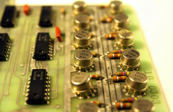
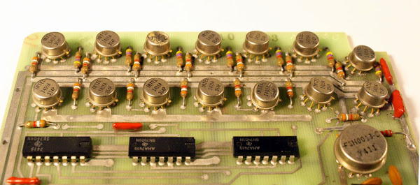
I got a display board from a Datapoint 2200[5], which uses Intel 1405 shift registers for the display storage. This board uses 14 shift registers and holds 896 bytes.[6] Shift-register memory was convenient for a video display board, since the circuitry needed to access each character in sequence to display it.
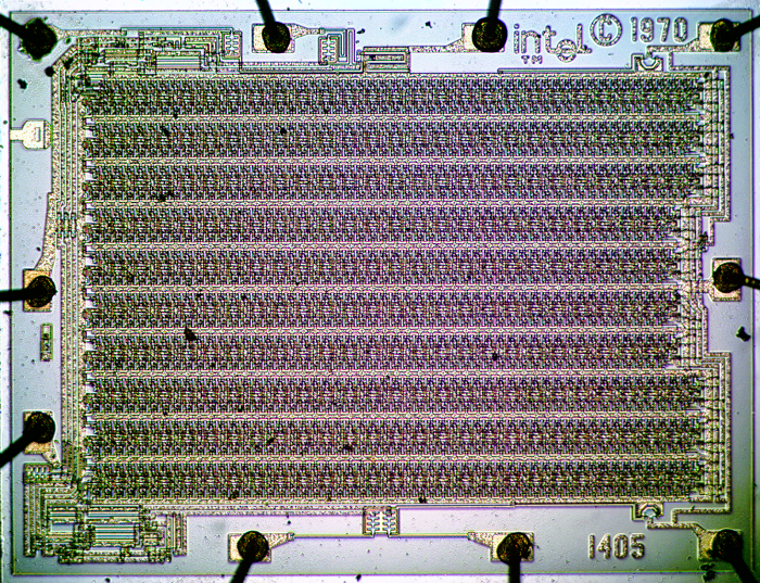
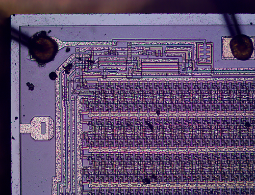
I opened up one of the shift register chips with a hacksaw and looked at it under a metallurgical microscope to get some die photos. Since the shift registers are in metal cans, they are easy to open up, unlike the plastic packages used by most chips. The following photo shows the die. The chip is fairly simple, with most of the chip taken up with the shift register cells. Around the outside of the chip you can see the nine pads with black wires connected.
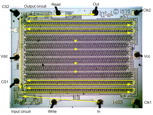
The die shows some of the reasons that shift registers were cheaper than RAM chips. Unlike a RAM chip, the chip does not need to form a regular grid — the rows in the middle are shorter than the others because of the pin on the right. In addition, the chip doesn't need any address decoding logic. Thus, more bits can be fit onto a chip. Because there are no address lines, the chip has fewer pins than a RAM chip and can fit into a smaller package.
The diagram below shows the flow of bits through the shift register, in yellow. Bits enter through the input pin at the bottom. They zig-zag through the 20 rows of the shift register and exit at the top through the output pin. Bits recirculate back to the input along the left. The clock lines are at the right and are connected to each cell of the shift register.
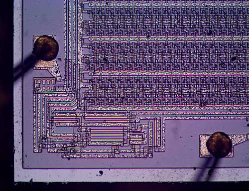
In the lower left is the circuit to control input to the shift register, which consists of a few gates. Either a new bit can be written to the shift register each cycle, or the exiting bit can recirculate and re-enter the shift register. The photo below zooms in on this circuit. The four vertical wires at the left are the chip select 2, chip select 1, recirculated bit, and Vdd.
The image below shows the circuit to control the output from the shift register, which is in the upper left of the chip. The chip has two chip select inputs, which makes it convenient to arrange the shift registers in a grid with one set of lines enabling a row and a perpendicular set of lines enabling a column.
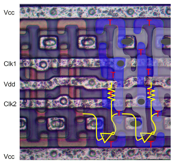
The large U shapes at the bottom are transistors (red T's) that form inverters (drawn in yellow). Between each inverter is a pass transistor that controls the flow of bits from inverter to inverter. The first T is connected to clock 1, allowing the bit to flow from the first inverter to the second when clock 1 is activated. The next T is connected to clock 2, passing the bit along another step on clock 2. As the clock lines are triggered in sequence, the bits pass step-by-step through the shift register.
The chip uses silicon-gate technology. This was an important innovation in chip design that was developed in 1968 at Fairchild by Federico Faggin (who also developed the Z80), and became a core technology at Intel. With this technology, polysilicon is used as the gates for transistors instead of aluminum metal, as previous MOS integrated circuits used. For various reasons, this made chips much faster and easier to manufacture.
In the picture below, polysilicon is indicated in blue. Where it overlaps the underlying doped silicon, a transistor is formed (red T). The horizontal gray lines are the metal layer, with the voltage supplies and the clocks. The circles show connections between the different layers.[7]
The clock driver
The display circuit board below has 14 shift registers in round metal cans. But there's a huge metal can at the right — what is this IC? That turns out to be the driver chip that provides the clock signals for the shift registers, and it's pretty interesting inside.The shift registers require two alternating clock signals to shift. These signals must not overlap, or else the data will get messed up. In addition, the shift registers require up to 30 volts in the clock, due to their old technology. Finally, a lot of current (500mA) is needed in the clock signals to drive all the chips. To meet these requirements, a special clock driver chip is used to generate the clock signals. This is the Fairchild SH0013-C "Two phase MOS clock driver".[8]
I expected to find an IC with big transistors inside the clock driver chip, but opening it up revealed something entirely different. Inside is a hybrid integrated circuit made up of eight separate silicon dies mounted on a tiny circuit board and connected with gold traces and gold wires. In addition, there are thick film resistors printed onto the board — these are the black "E" shapes in the picture below.
Interactive viewer
The image and schematic[8] below are an interactive exploration of the SH0013 clock driver. Click a component to see its location on the board and in the schematic highlighted. The box below will give an explanation of the component.
Conclusion
While using shift registers as memory seems bizarre now, it was a cost-effective way to implement storage in 1970. Looking inside the shift register chips shows how they work and how they could be implemented more cheaply than RAM. Providing the high-power clock signals required a special driver chip, which turns out to be a hybrid circuit with tiny semiconductors and resistors on a circuit board in a large metal IC package.Notes and references
[1] Intel didn't invent the memory chip, of course. There were many companies making memory chips in the 1960s. For instance, Texas Instruments announced the SN5481 bipolar memory chip in 1966 (Electronics, V39 #1, p151) and Transitron had the TMC 3162 and 3164 16-bit RAM (Electrical Design News, Volume 11, p14). In 1968, RCA made 72-bit CMOS memories for the Air Force (document, photo). Lee Boysel built 256-bit dynamic RAMs at Fairchild in 1968 and 1K dynamic RAMs at Four Phase Systems in 1969 (1970 — MOS Dynamic RAM Competes with Magnetic Core Memory on Price and Boysel presentation). For more information on the history of memory technology, see 1966 — Semiconductor RAMs Serve High-speed Storage Needs and History of Semiconductor Engineering, p215. Another source for memory history is To the Digital Age: Research Labs, Start-up Companies, and the Rise of MOS Technology, p193.[2] Memory chips started out very expensive, but prices rapidly dropped. Computer Design Volume 9 page 28, 1970, announced a price drop of the 3101 from $99.50 to $40 in small volumes. Electrical Design News Volume 15, 1970 gave the initial price of the 1405 as $13.30 in quantities of 100. Ironically, the Intel 3101 is now a collector's item and costs much more than the original price on eBay — hundreds of dollars for the right package.
[3] The datasheet for the 1405A shift register is available at Intel-vintage.info or Intel's data catalog 1976 (at archive.org).
[4] Many companies made shift register memories. For instance, in 1969 Philco (an electronics manufacturer owned by Ford Motor Company) claimed to have the longest commercially available shift register at 256 bits (Electronic Design, Volume 17, p251). For lots more information on shift register memory, see Don Lancaster's December 1974 Radio-Electronics article, " How it works: IC MOS shift registers.
[5] I obtained the Datapoint display board on eBay from Zuigadrummer, who currently has other Datapoint boards for sale. She was very helpful to me and I recommend her.
[6] The Datapoint 2200's display provided 12 lines of 80 characters. The display memory held 1024 7-bit ASCII characters. A pair of shift registers provided 1024 bits of storage, with 7 pairs in total.
[7] For those who want to know more details of the layout... The resistor symbols are not actually resistors, but clocked precharge transistors that pull the inverter outputs high. A few years later, MOS chips would use depletion transistors instead.
The metal rectangles form connections between the silicon layer and the polysilicon layer. This technique was soon obsoleted by buried contacts which connected the two layers directly without using the metal layer. This made chip layout easier, since the metal layer could be used for interconnections without being interrupted by these connections.
The gray blobs show the undoped silicon, which can be considered non-conductive. The doped silicon is conductive, except where the polysilicon crosses it and forms a transistor. Doped and undoped silicon are hard to distinguish in the die photo, but the boundary between them is visible as a faint black line. The polysilicon is much more visible in the die photo; it is orange, or red when it forms a transistor. The colors are due to the thicknesses of the layers.
[8] A datasheet for the SH0013 clock driver is in the 1973 Fairchild Linear Integrated Circuits Data Catalog, page 6-126. A datasheet for the equivalent MH0013 is in the 1972 National MOS Integrated Circuits databook, page 123.
Very interesting article I accidentally came across
ReplyDeleteNote that in describing the Datapoint 2200, it's the version 1 that was to use what ended being released as the Intel 8008.
About when intel was to deliver it, they said it would be a year more, Gary Asbel, Datapoint's hardware engineer used his serial design.
It still needed the 1103 shift registers. The design BTW, stores data in reverse order. IE data for 5, then 4, 3, 2, etc. is accessible. This made it slightly faster than storing in the expected 0, 1, 2, 3, etc order.
But now to my point.
The Version 1 2200 was quickly replaced by the version 2. New MSI circuits became available including RAM, rather than shift register memory. Though binary compatible, it had more instructions, a larger stack, and was much faster.
I have a similar board of unknown provenance with 20 rather than 14 Intel packages and empty spaces to accommodate another 10.
ReplyDeleteThe 8 pin TO-5 Intel packages are marked 335017 rather than 1405. Two DIP packages on the board have similar 6 digit numbers beginning with 3, so both are probably in-house numbers ordered by the manufacturer of the board, which also has such a 6 digit identifier 322956.
I must say, a hacksaw was not the tool I expected to be used to decap a chip.
ReplyDeleteHello~sir, I have a Datasheet PDF file for the SH0013 clock driver.
ReplyDeleteI split pages 6 through 126 into a small PDF file that from the 1973 Fairchild Linear Integrated Circuits Data Catalog.
Hoping to help others
Five years later, and I still have this shift register memory board.
ReplyDeleteLooking at
https://deramp.com/downloads/mfe_archive/050-Component%20Specifications/Intel/VintageIntelMicrochipsRev4.pdf
The twenty 8 pin integrated circuits on this board are either Intel i1401, i1402, i1403, or i1401 and were worth at least $20 each fifteen years ago. Is there a marketplace for these chips?
Contact me for photos of this board.