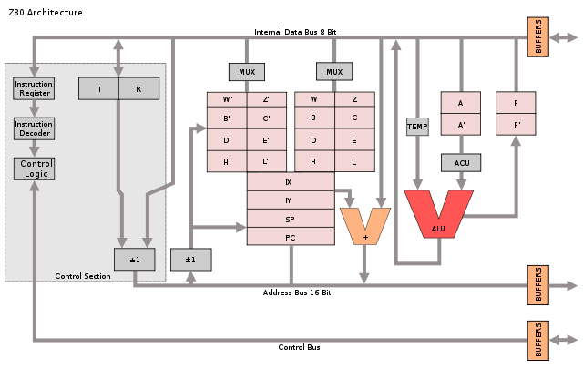
The Z80's architecture is often described with the diagram below, which shows the programmer's model of the chip.[1][2] But as we will see, the Z80's actual register and bus organization differs from this diagram in many ways. For instance, the data bus on the real chip has multiple segments. The diagram shows a separate incrementer for the refresh register (IR), an adder for IX and IY offsets, and a W'Z' register but those don't exist on the real chip. The Z80 shows that the physical implementation of a chip may be very different from how it appears logically.
Register overview and layout
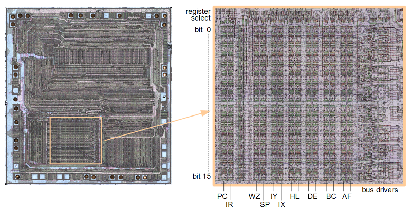
The diagram below shows how the Z80's registers are physically arranged on the chip, matching the die photo above. The register file consists of 14 pairs of 8-bit registers. In many cases, a pair of 8-bit registers is treated as a single 16-bit register. The bits are ordered from 0 at the top to 15 at the bottom, so the low-order byte is on the top and the high-order byte is on the bottom.At the right of the register file are the 8-bit accumulator (A) and 8-bit flag register (F). The accumulator holds the result of arithmetic and logic operations, so it is a very important register. The flag register holds condition flags, for instance indicating a zero value, negative value, overflow value or other conditions.
Note that there are two A registers and two F registers, along with two of BC, DE, and HL. The Z80 is described as having a main register set (AF, BC, DE, and HL) and an alternate register set (A'F', B'C', D'E', and H'L'), and this is how the architecture diagram earlier is drawn. It turns out, though, that this is not how the Z80 is actually implemented. There isn't a main register set and an alternate register set. Instead, there are two of each register and either one can be the main or alternate. This will be explained in more detail below.
To the left of the AF registers are the two general-purpose BC registers. These can be used as 8-bit registers (B or C), or a 16-bit register (BC). Next to them are the similar DE and HL registers. The HL register is often used to reference a location in memory; H holds the high byte of the address, and L holds the low byte. This register structure is based on the earlier 8080 microprocessor. (As will be explained later, DE and HL can swap roles, so these registers should really be labeled H/D and L/E.)
Next to the left are the 16-bit IX and IY index registers. These are used to point to the start of a region in memory, such as a table of data. The 16-bit stack pointer SP is to the left of the index registers. The stack pointer indicates the top of the stack in memory. Data is pushed and popped from the stack, for instance in subroutine calls. To the left of the stack pointer are the 8-bit W and Z registers. As will be discussed below, these are internal registers used for temporary storage and are invisible to the programmer.
Separated from the previous registers is the special-purpose memory refresh register R, which simplifies the hardware when dynamic memory is used.[3] The interrupt page address register I is below R, and is used for interrupt handling. (It provides the high-order byte of an interrupt handler address.)
Finally, at the left is the 16-bit PC (Program Counter), which steps through memory to fetch instructions. Since it is 16 bits, the Z80 can address 64K of memory. Its position next to the incrementer/decrementer is important and will be discussed below.
The Z80's register buses
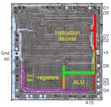
An important part of the Z80's architecture is how the registers are connected to other parts of the system by various buses. The Z80 is described as having a 16-bit address bus and an 8-bit data bus, but the implementation is more complicated.[3][4] The point of this complexity is to permit multiple register activities as the same time, so the chip can execute faster.The PC and IR registers are separated from the rest of the registers. As the diagram above shows, these registers are connected to the other registers through a 16-bit bus (thick black line). However, this bus can be connected or disconnected as needed (by pass transistors indicated by the vertical gray line). When disconnected, the PC and R registers can be updated while registers on the right are in use.
The internal register bus connects the PC and IR registers to an incrementer/decrementer/latch circuit. It has multiple uses, but the main purpose is to step the PC from one instruction to the next, and to increment the R register to refresh memory. The resulting address goes to the address pins via the address bus (magenta). I describe the incrementer/decrementer/latch in detail here.
At the right, separate 8-bit data buses connect to the low-order and high-order registers. These two buses can be connected or disconnected as needed. The lower bus (orange) provides access to the ALU (arithmetic logic unit). The upper bus (green) connects to another data bus (red) that accesses the data pins and instruction decoder.
Specifying registers in the opcodes
The Z80 uses 8-bit opcodes to specify its instructions, and these instructions are carefully designed to efficiently specify which registers to use. Register instructions normally use three bits to specify the register used:000=B, 001=C, 010=D, 011=E, 100=H, 101=L, 110=indirect through HL, 111=A.[5]
For instance, the ADD instructions have the 8-bit binary values 10000rrr, where the rrr bits specify the register to use as above.
Note that in this pattern the two high-order bits specify the register pair, while the low order bit specifies which half of the pair to use; for example 00x is BC, 000 is B, and 001 is C. For instructions operating on a register pair (such as 16-bit increment INC), the opcode uses just the two bits to specify the pair.
By using this structure for opcodes, the instruction decoding logic is simplified since the same circuitry can be reused to select a register or register pair for many different instructions. Instruction decode circuitry located above the register file uses the two bits to select the register pair and then uses the third bit to pick the lower or upper half of the register file.
The register selection bits can be in bits 2-0 of the instruction, for example AND; in bits 5-3 of the instruction, for example DEC (decrement); or in both positions, for example register-to-register LD.[6]
To handle this, a multiplexer selects the appropriate group of bits and feeds them into the register select logic. Thus, the same circuit efficiently handles register bits in either position. By designing the instruction set in this way, the Z80 combines the ability to use a large register set with a compact hardware implementation.
Swapping registers through register renaming
The Z80 has several instructions to swap registers or register sets. TheEX DE, HL instruction exchanges the DE and HL registers. The EX AF, AF' instruction exchanges the AF and AF' registers.
The EXX instruction exchanges the BC, DE, and HL registers with the BC', DE', and HL' registers.
These instructions complete very quickly, which raises the question of how multiple 16-bit register values can move around the chip at once.
It turns out that these instructions don't move anything. They just toggle a bit that renames the appropriate registers. For example, consider exchanging the DE and HL registers. If the DE/HL bit is set, an instruction acting on DE uses the first register and an instruction acting on HL uses the second register. If the bit is cleared, a DE instruction uses the second register and a HL instruction uses the first register. Thus, from the programmer's perspective, it looks like the values in the registers have been swapped, but in fact just the meanings/names/labels of the registers have been swapped. Likewise, a bit selects between AF and AF', and a bit selects between BC, DE, HL and the alternates. In all, there are four registers that can be used for DE or HL; physically there aren't separate DE and HL registers.
The hardware to implement register renaming is interesting, using four toggle flip flops.[7] These flip flops are toggled by the appropriate EX and EXX instructions. One flip flop handles AF/AF'. The second flip flop handles BC/DE/HL vs BC'/DE'/HL'. The last two flip flops handle DE vs HL and DE' vs HL'. Note that two flip flops are required since DE and HL can be swapped independently in either register bank.
The flags
The flags have a dual existence. The flags are stored inside the register file, but at the start of every instruction,[8] they are copied into latches above the ALU. From this location, the flags can be used and modified by the ALU. (For example, add or shift operations use the carry flag.) At the end of an instruction that affects flags, the flags are copied from the latches back to the register file.Most of the flags are generated by the ALU (details here). The circuitry to set and use the carry is complicated, since it is used in different ways by shifts and rotates, as well as arithmetic. Conditional operations are another important use of the flags.[9]
The WZ temporary registers
The Z80 (like the 8080 and 8085) has a WZ register pair that is used for temporary storage but is invisible to the programmer. The primary use of WZ is to hold an operand from a two or three byte instruction until it can be used.[10]
The JP (jump) instruction shows why the WZ registers are necessary. This instruction reads a two-byte address following the opcode and jumps to that address. Since the Z80 only reads one byte at a time, the address bytes must be stored somewhere while being read in, before the jump takes place. (If you read the bytes directly into the program counter, you'd end up jumping to a half-old half-new address.) The WZ register pair is used to hold the target address as it gets read in. The CALL (subroutine call) instruction is similar.
Another example is EX (SP), HL which exchanges two bytes on the stack with the HL register. The WZ register pair holds the values at (SP+1) and (SP) temporarily during the exchange.
How the registers are implemented in silicon
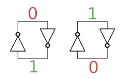
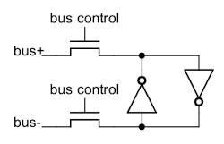
The building block for the registers is a simple circuit to store one bit, consisting of two inverters in a feedback loop. In the diagram below, if the top wire has a 0, the right inverter will output a 1 to the bottom wire. The left inverter will then output a 0 to the top wire, completing the cycle. Thus, the circuit is stable and will "remember" the 0. Likewise, if the top wire is a 1, this will get inverted to a 0 at the bottom wire, and back to a 1 at the top. Thus, this circuit can store either a 0 or a 1, forming a 1-bit memory.[11]
How does a value get stored into this inverter pair? Surprisingly, the Z80 just puts stronger signals on the wires, forcing the inverters to take the new values.[12] There's no logic involved, just "might makes right". (In contrast, the 6502 uses an additional transistor in the inverter feedback loop to break the feedback loop when writing a new value.)
To support multiple registers, each register bit is connected to bus lines by two pass transistors. These transistors act as switches that turn on to connect one register to the bus. Each register has a separate bus control signal, connecting the register to the bus when needed. Note that there are two bus lines for each bit - the value and its complement. As explained above, to write a new value to the bit, the new value is forced into the inverters. There are 16 pairs of bus lines running horizontally through the register file, one for each bit.
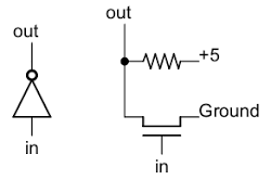
Next, to see how an inverter works, the schematic below shows how an inverter is implemented in the Z80. The Z80 uses NMOS transistors, which can be viewed as simple switches. If a 1 is input to the transistor's gate, the switch closes, connecting ground (0) to the output. If a 0 is input to the gate, the switch opens and the output is pulled high (1) by the resistor. Thus, the output is the opposite of the input.[13]
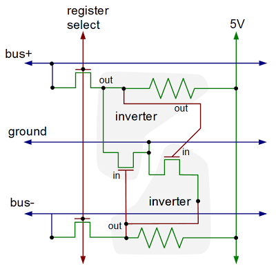
Putting this all together - the two inverters and the pass transistors - yields the following schematic for a single bit in the register file. The layout of the schematic matches the actual silicon where the inverters are positioned to minimize the space they take up. The bus lines and ground run horizontally. The control line to connect a register to the buses runs vertically, along with the 5V power line.
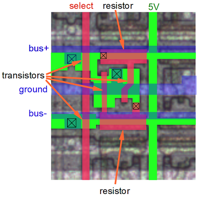
The diagram below shows the physical implementation of a register bit in the Z80, superimposed on a photo of the die. It's tricky to understand this, but comparing with the schematic above should help. The silicon is in green, the polysilicon is in red, and the metal lines are in blue. Transistors occur where the polysilicon (red) crosses the silicon (green). The X in a box indicates a contact connecting two layers. Note the large area taken up by the resistors (which are formed from depletion-mode transistors). Additional register bits can be seen in the photo, surrounding the bit illustrated.
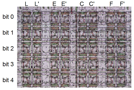
Zooming out, the picture below shows the upper right part of the register file. Each bit consists of a structure like the one above. Each column is a separate register, with a separate control line, and each row is one of the bits. The columns are in groups of two, with the register control lines between the pairs of columns. Zooming out more, the image at the top of the article shows the full register file and its location in the chip. Thus, you can see how the entire register file is built up from simple transistors.
Comparison with the 6502 and 8085
While the Z80's register complement is tiny compared to current processors, it has a solid register set by 1976 standards - about twice as many registers as the 8085 and about four times as many registers as the 6502. Because they share the 8080 heritage, many of the 8085's registers are similar to the Z80, but the Z80 adds the IX and IY index registers, as well as the second set of registers.The physical structure of the Z80's register file is similar to the 8085 register file. Both use 6-transistor static latches arranged into a 16-bit wide grid. The 8085, however, uses complex differential sense amplifiers to read the values from the registers. The Z80, by contrast, just uses regular gates. I suspect the 8085's designers saved space by making the register transistors as small as possible, requiring extra circuitry to read the weak values on the bus lines.
The 6502, on the other hand, doesn't have a separate register file. Instead, registers are put on the chip where it turns out to be convenient. Since the 6502 has fewer registers, the register circuitry doesn't need to be as optimized and each bit is more complex. The 6502 adds a transistor to each bit so it is clocked, and separate pass transistors for read and write. One consequence is direct register-to-register transfers are possible on the 6502, since the source and destination registers can be distinguished. Instead of a separate incrementer unit, the 6502's program counter is tangled in with the incrementer circuitry.
Conclusion
By looking at the silicon of the Z80 in detail, we can determine exactly how it works. The Z80's register file has more complexity than you'd expect and the hardware implementation is different from published architecture diagrams. By splitting the register file in two, the Z80 runs faster since registers can be updated in parallel. The Z80 includes a WZ register pair for temporary storage that isn't visible to the programmer. The Z80's register storage has many similarities to the 8085, both in the registers provided and their hardware implementation, but is very different from the 6502.Credits: This couldn't have been done without the Visual 6502 team especially Chris Smith, Ed Spittles, Pavel Zima, Phil Mainwaring, and Julien Oster. All die photos are from the visual 6502 team.
Notes and references
[1] There are many variants of that architecture diagram; the one above is from Wikipedia. The original source of the common Z80 architecture diagram is the book Programming the Z80 by Rodnay Zaks, page 65 (HTML or PDF). The book is an extremely detailed guide to the Z80, down to the instruction cycles. I don't mean to criticize the architecture diagram by pointing out differences between it and the actual silicon. After all, it is a logic-level diagram intended for use by programmers, not a hardware reference. But it is interesting to see the differences between the programmer's view and the hardware implementation.[2] Zilog's Z80 CPU user manual is a key reference on the instruction set and operation of the Z80, but it doesn't provide any information on the internal architecture.
[3] The Z80's memory refresh feature is described in patent 4332008. Figure 15 in the patent shows the segmented data bus used by the Z80, although it is a mirror image of the actual die.
[4] I wrote more about the data buses in the Z-80 in Why the Z-80's data pins are scrambled.
[5]
The bit pattern 110 is an exception to the encoding of registers in instructions, since it refers to a memory location indexed by the HL register pair, rather than a register.
Likewise the bit pattern 11x referring to a register pair is also an exception. It can indicate the SP register, for example in 16-bit LD, INC and DEC instructions.
[6] The Z80 specifies registers in instruction bits 0-2 and bits 3-5. This maps cleanly onto octal, but not hexadecimal. One consequence is the opcodes are more logical if you arrange them in octal (like this), instead of hexadecimal (like this). Perhaps the designers of the Z80 were thinking in octal and not hex.
[7] The toggle flip flops are unlike standard flip flops formed from gates. Instead they use pass transistors; this lets it hold the previous state while toggling to avoid oscillation. Because the pass transistor circuits depend on capacitance holding the values, you have to keep the clock running. This is one reason the clock in the Z80 can't stop for more than a couple microseconds. (The CMOS version is different and the clock can stop arbitrarily long.) From looking at the silicon, it appears that these flip flops required some modifications to work reliably, probably to ensure they toggled exactly once.
These flip flops have no reset logic, so it is unpredictable how the registers get assigned on power-up. Since there's no way to tell which register is which, this doesn't matter.
The active DE vs HL flip flop swaps the DE and HL register control lines using pass-gate multiplexers. The main vs alternate register set flip flops direct each AF/BC/DE/HL register control line to one of the two registers in the pair.
[8] Like many processors of its era, the Z80 starts fetching a new instruction before the previous instruction is finished; this is known as fetch/execute overlap. As a result, the flags are actually written from the latches to the register file three cycles into the next instruction (i.e. T3), and the flags are read from the register file into the latches four cycles into the instruction (i.e. T4).
[9]
I'll explain briefly how conditional instructions such as jump (JP) work with the flags.
Bits 4 and 5 of the opcode select the flag to use (via a multiplexer just to the right of the registers).
Bit 3 of the opcode indicates the desired value (clear or set); this bit is XORed with the selected flag's value. The result indicates if the desired condition is satisfied or not, and is fed into the control logic to determine the appropriate action. The JR and DJNZ don't exactly fit the pattern so a couple additional gates adjust their bits to pick the right flags.
[10] For more explanation of the WZ registers, see Programming the Z80, pages 87-91.
[11] The register storage in the Z80 is called "static" memory, since it will store data as long as the circuit has power. In contrast, your computer uses dynamic memory, which will lose data in milliseconds if the data isn't constantly refreshed. The advantage of dynamic memory is it is much simpler (a transistor and a capacitor), and thus each cell is much smaller. (This is how DRAM can fit gigabits onto a single chip.) Another alternative is flash memory, which has the big advantage of keeping its contents while the power is turned off.
[12] If you've built electronic circuits, it may seem dodgy to force the inverters to change values by overpowering the outputs. But this is a standard technique in chips. To understand what happens, remember that in an NMOS circuit, a 0 output is created by a transistor to ground, while a 1 output is made by a much weaker resistor. So if one of the inverters is outputting a 1 and a 0 is connected to the output, the 0 will "win". This will cause the other inverter to immediately switch to 1. At this point, the original inverter will switch to output 0 and the inverter pair is now stable with the new values.
To improve speed, and to prevent a low voltage on the bus from accidentally clearing a bit while reading a register, the bus lines are all precharged to +5 every clock cycle. A low output from an inverter will have no trouble pulling the bus line low, and a high output will leave the bus line high. The precharging is done through transistors in the space between the IR and WZ registers.
[13] One disadvantage of NMOS logic is the pull-up resistors waste power. In addition, the output is fairly slow (by computer standards) to change from 0 to 1 because of the limited current through the resistor. For these, reasons, NMOS has been almost entirely replaced by CMOS logic which instead of resistors uses complementary transistors to pull the output high. (As a result, CMOS uses almost no power except while switching outputs from one state to another. For this reason, CMOS power usage scales up with frequency, which is why CPUs are hitting clock limits - they're too hot to run any faster.)

21 comments:
Hi, I enjoyed reading your treatise on the Z80. Have you by any chance seen the following book: "The architecture of microprocessors" by Francois Anceau?
It contains a very nice chapter on the internal architecture of the Motorola MC68000 and if I remember correctly it also includes some information about the Z80 processor which you might be interested in reading.
Such a great processor. Gives me warm feelings.
Here you can look at the totally revengineered 580BM80A (soviet clone of Intel 8080A) - complete (transistor level) schematic and Verilog code, running on the Altera DE0 board
http://zx-pk.ru/showthread.php?t=23349
It seems the 8080A shares a lot with Z80.
I really like that ! thanks !
How did you learn to reverse engeneer a processor,and all that stuff ?
thanks for replying ;)
Ken, I've used your Arduino libraries in the past, but only recently stumbled upon your blog. What an incredible series of articles on 70's electronics! They should be required reading for any electronics under-grad. There was a lot of government surplus electronic stuff available in the UK in the 70's and I well remember popping the lids of ceramic ICs and examining them with a microscope. Excellent body of work! Derek (retired electronics engineer)
I’m fixing the emulation of resets in an emulation of the Z80, and would like to know: AF is set to $FFFF upon reset, but is AF' too?
I figure both AF registers ("AF and AF'") must be cleared upon reset, unless the AF renaming flip-flop is itself reset upon a reset. Even if nobody knows, I'd be interested in thoughts as to the likely behaviour. Any ideas?
I remember when I got a ZX81, after playing with Basic I looked at the Z80 opcode list at the end of the manual, and I thought "this looks like fun".
I bought a Z80 book by zilog, and it was fun ! What a great processor !
The 6502 uses an addressable-register architecture, and basically all of zero page is 256 bytes of processor registers. Loads from, or stores to, these 256 takes three clocks (T-states in the parlance of other processors), and doing indirects or indexing may add to those; so for example LDA ZP,X (load accumulator register from a zero page address indexed by the contents of the X register) takes four clocks. The fastest 65c02's today are running over 200MHz (about 50MIPS). There is minor pipelining, so for example ADC#14 (add with carry, immediate, a 14), carries out five distinct steps in 2 clocks.
Western Design Center licenses the IP to client companies who put it at the heart of custom ICs for automotive, industrial, appliance, toy, and even life-support products, at a rate of a hundred million units a year, even now in 2015.
Thanks for the nostalgic trip back to 80's... :-) Vlada
Many thanks for a great article.
Is one able to load a 16 bit register pair directly with the contents of the PC (without the presence of any external RAM)?
Do we know in which manufacturing process the Z80A die was made? ...or even the minimum gate length. I'm working a spice model of the output driver of the address lines. Thank you.
@Dan Moore
According to https://zeptobars.com/en/read/Zilog-Z80-Z0840004PSC the die size is 3545x3350 µm. Using that information and their die shot you should be able to figure that out. (Yes, I know it will be a real pain in the ass—but at least you'll have the critical scaling measurement to start with.)
@Stuart Brady
How many times do those of us trained in hardware design have to remind programmers that uninitialized registers should always be assumed to contain random garbage? I strongly suspect what _really_ happens is that AF contains trash at power-up and the first few internal actions needed to load in the first instruction incidentally put 0xFFFFh into AF. (Remember as well that only 6 bits of F have meaning...)
@ Drew Northup
Oh, it can be the other way around too. As a mixed-signal verification engineer, I've corrected many of analog designers' models that magically initialize themselves to zero. "...but that's how it comes up in my SPICE simulation!" No, no.
Anyway, Sean Young's document here: http://www.z80.info/zip/z80-documented.pdf .states that AF "[is] always set to FFFFh after reset" citing the research work of "Matt". (sorry no mention of AF') I'm still a bit skeptical. The email address for Matt is dead.
Since posting, I had made some headway with the SPICE netlist and device model. I did as you suggested, got out the ruler and started measuring and scaling. It appears that the NMOS device lengths are 10um. Although I haven't discovered the exact device models for both the enhancement and depletion type nfets, I did come across suitable stand ins. ...and backward engineering the schematic from the layout wasn't too bad. I'll share if anyone's interested.
Ken, have you ever decoded the 16-bit register ALU that sits between the Z80’s register file and address bus? It’s appears in most Z80 block diagrams. It seems to be a 16-bit adder, likely used to perform the IX+d, IY+d and PC+e operations (adding a signed 8-bit displacement on the data bus to the selected 16-bit register before gating the result onto the address bus).
Based on the block diagrams I’ve seen, it appears that all selected 16-bit registers pass through this ALU on their way to the address bus; the register passes through the ALU unchanged except for the add operations mentioned above.
I’d certainly enjoy learning more about this circuit if you have any insights.
And thanks for your excellent work in help unravel the Z80’s internal architecture!
Thank you! "In the days" I was programming Z80 for money, e.g. a 32bit integer math package with fast ASCII decimal to binary routines in assembler. I did not understand why the INC HL opcode (1 M cycle, 6 T states) does not set the carry or zero flag, but the INC A opcode (1 M cycle, 4 T states) does. I assume that the "16bit incrementer" has no logic to set carry or zero flag. By why is INC HL a 6 T state opcode? I always thought that low byte was incremented by the ALU in 4 T states and the maybe necessary high byte increment was done in the last 2 T states.
Thank you for the great blog! The content is really insightful.
I have a short question regarding the figure depicting the physical register implementation on the die: https://static.righto.com/images/z80/register_cell2.png
I'm not quite sure, but is there a contact for the lower pull-up resistor to the poly silicon in this image missing?
Anonymous: the lower pull-up resistor has a contact in the upper right, above the main rectangle.
Follow-up for the pull-up resistor question: Yes, I have seen this contact. My question is if there is a second contact required on the left side of this poly-silicon to the lower silicon layer.
As far as I understood the bottom silicon line (green) forms a transistor that acts like a resistor with the poly-silicon above (red). Which means that the left side of the silicon line will be the first end of the resistor while the other one is at the 5V line to the right. How is this left end of the resistor now connected to the base of the inverter above (on the central left of the main rectangle)?
From this figure I got the impression that those two might need a connection from the poly-silicon to the silicon line below on the left:
https://static.righto.com/images/z80/register_bit_schematic.png
Anonymous: I see what you mean now. Yes, you are correct. I missed the contact there.
Hi everybody,
I got a ZX81 in the mid 80's for about 120DM and was fascinated.
Soon I figured out the Z80 opcode and how to get it in the little machine,
you have to write your code as hexnibbles in Basic remlines and start it somehow.Forgotten.
And so I knew the whole Z80 opcode in hex, assembler was in my brain.
It's long, long fun time ago nothing of that remains.
Grüße,
Uwe
Ken,
Another excellent post in your continuing series of reverse engineering common microprocessors.
You said:
[6] The Z80 specifies registers in instruction bits 0-2 and bits 3-5. This maps cleanly onto octal, but not hexadecimal. One consequence is the opcodes are more logical if you arrange them in octal (like this), instead of hexadecimal (like this). Perhaps the designers of the Z80 were thinking in octal and not hex.
This is likely because the Z80 had to retain instruction compatibility with at least most of the first 256 opcodes of the 8080 and 8085.
The 8080 architecture dates from the very early 1970s and shares some commonality with the earlier 8008, and the Datapoint 2200. At the time these processors were designed, octal was very much the standard, with hex only starting to appear in some 16-bit minicomputers.
However, to my knowledge both the 6800 and it's "spin-off" the 6502 have instruction sets that have encoding that makes more sense when expressed in hex.
Post a Comment