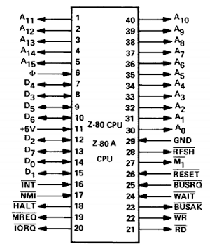
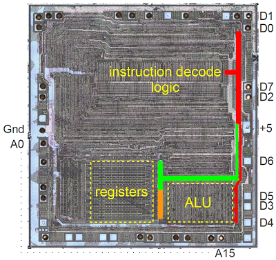
I have been reverse-engineering the Z-80 processor using images and data from the Visual 6502 team. The image below is a photograph of the Z-80 die. Around the outside of the chip are the pads that connect to the external pins. (The die photo is rotated 180° compared to the datasheet pinout, if you try to match up the pins.) At the right are the 8 data pins for the Z-80's 8-bit data bus in a strange order.
The 8-bit data bus in the Z-80 is used for communication among the different parts of the chip. But instead of a single data bus, the Z-80 has a complex data bus that is split into 3 segments. The first segment of the data bus (in red) connects to the data pins to the instruction decode logic. The first segment is also connected to the second segment (green). The green data bus provides access to the lower byte of registers and is also connected to the fourth segment of the data bus (orange). The orange data bus is connected to the high byte of registers and also to the ALU (Arithmetic Logic Unit)[2]. Note that because the green segment splits off from the red segment, only half of the red bus (4 bits) goes down to the lower part of the chip. [There was an extra segment in an earlier version of this article.]
The motivation behind splitting the data bus is to allow the chip to perform activities in parallel. For instance an instruction can be read from the data pins into the instruction logic at the same time that data is being copied between the ALU and registers. The partitioned data bus is described briefly in the Z-80 oral history[3], but doesn't appear in architecture diagrams.
The complex structure of the data buses is closely connected to the ordering of the data pins. But before explaining the data pin layout, a few more features of the Z-80 need to be discussed.
How the Z-80 processes instructions
To execute an instruction, the Z-80 loads the instruction from memory through the data pins and feeds it into the instruction decode logic via the red segment of the data bus. First, the instruction is stored from the data bus into the instruction register, which is a simple latch that holds the instruction while it is being executed. This feeds the instruction into the PLA (Programmable Logic Array), which decodes the instruction into approximately 98 different categories (details). The instruction logic below the PLA combines these signals with timing signals and determines exactly what should happen at what step. This logic generates the control signals that control the operation of the register file, ALU, and other parts of the chip.Since the Z-80 is an 8-bit processor, instruction op codes are 8 bits long. Many of the instructions have the bits arranged as follows:
ggiiirrr
In that arrangement, the two gg bits select a group of instructions (e.g. load or arithmetic), the next three iii bits select the particular instruction, and the last three rrr bits select the register to use. There are many exceptions to this format, but it provides an underlying structure. (This instruction structure was inherited from the 8080 microprocessor, since the Z-80 was designed to be backwards compatible with it.)
Bit instructions in the Z-80
One feature the Z-80 has that goes beyond the 8080 is instructions to set, clear, or test a single bit in a register.[4] These instructions fit the pattern described above, with the top two bits in the instruction selecting the test, clear, or set function, the next three bits in the instruction selecting which bit in the byte to operate on, and the final three bits selecting the register. That is, bits 5, 4, and 3 of the instruction select which of the eight bits in the register to operate on.The processing of the Z-80's bit operations is unusual compared to other instructions. While most of the instruction execution is controlled by the same instruction decoding logic described above, the bit selection is done by feeding the three instruction bits directly into the ALU, bypassing the instruction decoding logic entirely. That is, there are simple circuits (at the right side of the ALU) to select one of the 8 bits, depending on the instruction that was read in. In the diagram of the chip, you can see the connection between the data bus (red) and the ALU to accomplish this.
The hardware to do the bit selection is fairly straightforward. There are eight 3-input NOR gates, each looking at a different combination of the instruction bits, either inverted or non-inverted. For example, an instruction that operates on bit 2 will have an opcode of the form gg010rrr (since 010 is binary 2). Instruction bit 5 is 0, instruction bit 4 is 1, and instruction bit 3 is 0. (Don't confuse the bits in the instruction with the bit being selected.) In logic, this becomes:
modify_data_bit_2 = (NOT bit5) AND bit4 AND (NOT bit3).
It turns out that NOR gates are easiest to build in silicon (as will be explained below), so the logic in hardware is the equivalent:
modify_data_bit_2 = bit5 NOR (NOT bit4) NOR bit3.
Selection of the other 7 bits is done with similar functions of the instruction bits bit5, bit4, and bit3.
The hardware implementation of bit instructions
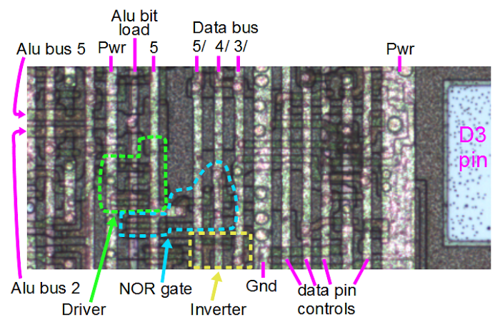
For a bit operation, one of the 8 bits will be selected and fed into the ALU. The ALU will then test, clear, or set that bit in the appropriate register. Below is a zoomed-in look at the portion of the die that selects bit 2. This is in the lower right corner of the chip, to the right of the ALU by the D3 pad. The white vertical stripes are metal lines, providing the data lines, control lines, and power and ground. Underneath the metal is the polysilicon layer. Underneath this is silicon layer, where the transistors are. It's hard to make out the polysilicon and silicon structures in this photo, but at the left you can see the horizontal polysilicon bus lines for ALU bits 5 and 2. These lines provide data flow through the ALU, and are how the selected bit is fed into the ALU.
The data bus provides bits 5, 4, and 3 to this part of the chip. (Just to make thing confusing, the data on the Z-80's data bus is inverted, which is indicated by a slash.) Underneath this bus is the NOR gate (outlined in blue) that computes the function described earlier: bit5 NOR (NOT bit4) NOR bit3. The inverter to bit3 from the inverted bit3 on the data bus is also visible (outlined in yellow). A buffer (green) strengthens this signal.
The "ALU load bit value" control line is activated by the instruction decode logic; this control line allows the selected bit to pass into the ALU only for a bit operation.
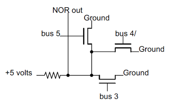
A NOR gate is a simple circuit when implemented with MOS transistors, as the schematic below shows. The transistors can be thought of as switches that close if their gate (middle connection) receives a 1 input. In the circuit below, if any of the inputs are 1, the corresponding transistor will connect the output to ground, and the output will be 0. Otherwise, the resistor (which is actually a special depletion-mode transistor) will pull the output high and the output is 1. Thus, the output is the NOR of the three inputs.
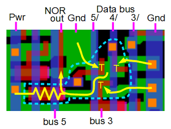
The diagram below shows how the above NOR gate is actually implemented in silicon. The diagram is a zoomed-in version of the image above, focusing on the NOR gate (blue outline). Instead of a photograph, the diagram shows the different layers in the chip as extracted by the Visual 6502 team: blue is metal, brown is polysilicon, green is silicon, and orange is a connection between layers. A transistor is formed when polysilicon crosses silicon.
The "T" symbols indicate the three transistors that are connected to ground (as shown by yellow arrows). The transistors are all connected together in the middle, and the final yellow arrow shows the connection to the output. Finally, the pull-up resistor is at the lower left. The cyan outline matches the outline in the die photo and with difficulty you can find the structures in the photo.
The important thing to notice in the diagram above is that everything is packed together as tightly as possible to get the Z-80 to fit on the available silicon. The layout of the Z-80 was done by hand, with each transistor and connection manually positioned. Every possible trick was used to minimize space - for example, each transistor above is oriented in a different direction. Drafting this layout was an extremely time-consuming task that took Zilog founder Federico Faggin 3 1/2 months of 80-hour weeks[3]. (Yes, the CEO drafted the chip himself!) But you can see from the result that there is very little wasted space in the chip.
The data pins
This article has looked at many different aspects of the Z-80 design, and now it's time to see how they constrain the position of the data pins. First, because the Z-80 splits the data bus into multiple segments, only four data lines run to the lower right corner of the chip. And because the Z-80 was very tight for space, running additional lines would be undesirable. Next, the BIT instructions use instruction bits 3, 4, and 5 to select a particular bit. This was motivated by the instruction structure the Z-80 inherited from the 8080. Finally, the Z-80's ALU requires direct access to instruction bits 3, 4, and 5 to select the particular data bit. Putting these factors together, data pins 3, 4, and 5 are constrained to be in the lower right corner of the chip next to the ALU. This forces the data pins to be out of sequence, and that's why the Z-80 has out-of-order data pins.[5]Credits: The chip analysis couldn't have been done without the Visual 6502 team especially Chris Smith, Ed Spittles, Pavel Zima, Phil Mainwaring, and Julien Oster.
Notes and references
[1] Even though the Z-80 has out-of-order data pins, it is an improvement over the 8080, where both address and data pins are in a strange order. The 6502, on the other hand, has a nice linear order for its pins.[2] Unexpectedly, the Z-80's ALU is 4 bits wide. I've written up details here.
[3] The Computer History Museum created an oral history of the Z-80, which is very interesting. A couple parts of it are especially relevant to this article. Page 10 discusses the segmented data bus. Pages 5, 9, and 19 discuss Zilog CEO Federico Faggin laying out the chip over several months. One interesting story is how he ran out of room and had to erase two weeks of work and start over. In the end he completed the layout with only a couple mils of space left.
[4]
The Z-80 has multiple operations to set, clear, or test a single bit.
These instructions are expressed by two bytes. The first byte is the prefix CB, and the second byte is the specific instruction.
The top two bits (ii) of the instruction are 01 for BIT (test bit), 10 for RES (reset bit), and 11 for SET (set bit).
For more details, see the Z-80 User Manual, page 240.
[5] Even with pins 3, 4, and 5 out of order, the Z-80 could have used a "semi-linear" sequence such as 0,1,2,6,7,3,4,5. Why didn't the Z-80 do this? My hypothesis is that once some pins were forced out of sequence, the Z-80's designers decided to take advantage of any other micro-optimizations from reordering the pins. For example, pins D0 and D1 have their drivers in order on the chip, but the routing from the drivers to the pins swaps the order to avoid crossing. Pin D7 is probably where it is because its driver lines up well with bit 7 in the PLA. Switching the positions of pins D3 and D4 would make the routing a tiny bit longer.
Great to see the ole fella had not been forgotten Ken. I cut my teeth in the z80 (hardware and software) and s/he launched me on a fun and successful career. Nice to see the point again and peek inside for the first time :-)
ReplyDeleteHi Ken,
ReplyDeleteThanks for a great article.
The link to Z80_arch.svg has no quotation mark before the URL, but has one after the URL. This makes Google Chrome go to a wrong URL (ending in a quotation mark), which gives the user a 404 page.
Kind regards,
Morten
Awesome article, with a whole load of effort behind it. Way to go!
ReplyDeleteYou might find this interesting I'm not sure I completely like your definition of rrr in ggiiirrr
ReplyDeleteIts been a few years since I wrote this and I hope you can make sense of the VAX-11 macro
This emulator was written a long time a go and my bios is missing but at one time it would boot to an :\ thought not bug free or perfect it is different to most Z80 emulators in that it looks at the bit of the opcode rather then just a simple lookup table
https://github.com/gcsgithub/z80_vax11/blob/master/z80.mar
Foarte interessnt
ReplyDelete