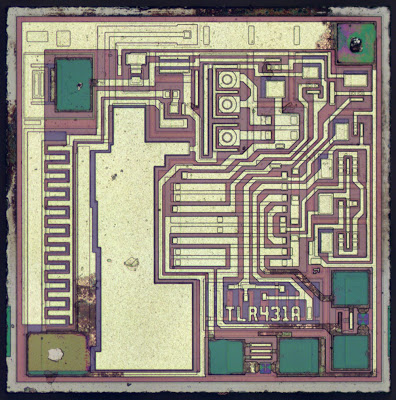
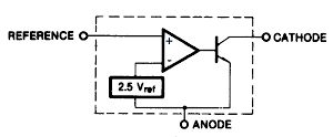
The TL431 is a "programmable precision reference"[1] and is commonly used in switching power supplies, where it provides feedback indicating if the output voltage is too high or too low. By using a special circuit called a bandgap, the TL431 provides a stable voltage reference across a wide temperature range. The block diagram of the TL431 below shows that it has a 2.5 volt reference and a comparator[1], but looking at the die shows that internally it is quite different from the block diagram.
The TL431 has a long history; it was introduced in 1978[2] and has been a key part of many devices since then. It helped regulate the Apple II power supply, and is now used in most ATX power supplies[3] as well as the the iPhone charger and other chargers. The MagSafe adapter and other laptop adapters use it, as well as minicomputers, LED drivers, audio power supplies, video games and televisions.[4]
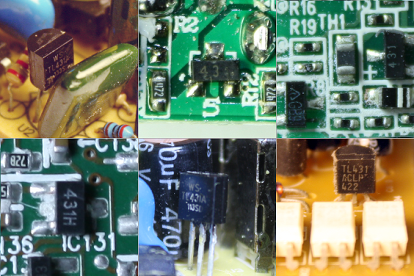
The photos below show the TL431 inside six different power supplies. The TL431 comes in many different shapes and sizes; the two most common are shown below.[5] Perhaps a reason the TL431 doesn't get much attention because it looks like a simple transistor, not an IC.
How components are implemented in the TL431's silicon
Since the TL431 is a fairly simple IC, it's possible to understand what's going on with the silicon layout by examining it closely. I'll show how the transistors, resistors, fuses, and capacitors are implemented, followed by a reverse-engineering of the full chip.Implementing different transistor types in the IC
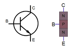
The chip uses NPN and PNP bijunction transistors (in contrast to chips like the 6502 that use MOSFET transistors). If you've studied electronics, you've probably seen a diagram of a NPN transistor like the one below, showing the collector (C), base (B), and emitter (E) of the transistor, The transistor is illustrated as a sandwich of P silicon in between two symmetric layers of N silicon; the N-P-N layers make a NPN transistor. It turns out that on the chip, the transistors look nothing like this. The base isn't even in the middle!
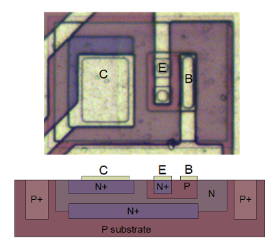
The photo below shows one of the transistors in the TL431 as it appears on the chip. The different pink and purple colors are regions of silicon that has been doped differently, forming N and P regions. The whitish-yellow areas are the metal layer of the chip on top of the silicon - these form the wires connecting to the collector, emitter, and base.
Underneath the photo is a cross-section drawing showing approximately how the transistor is constructed.[6] There's a lot more than just the N-P-N sandwich you see in books, but if you look carefully at the vertical cross section below the 'E', you can find the N-P-N that forms the transistor. The emitter (E) wire is connected to N+ silicon. Below that is a P layer connected to the base contact (B). And below that is a N+ layer connected (indirectly) to the collector (C).[7] The transistor is surrounded by a P+ ring that isolates it from neighboring components. Since most of the transistor in the TL431 are NPN transistors with this structure, it's straightforward to pick out the transistors and find the collector, base, and emitter, once you know what to look for.
The NPN output transistor in the TL431 is much larger than the other transistors since it needs to handle the full current load of the device. While most of the transistors are operating on microamps, this transistor supports up to 100 mA. To support this current, it is large (taking up more than 6% of the entire die), and has wide metal connections to the emitter and collector.
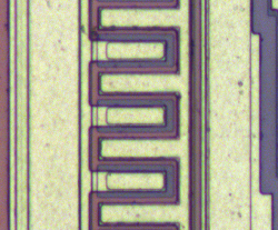
The layout of the output transistor is very different from the other NPN transistors. This transistor is built laterally, with the base between the emitter and collector. The metal on the left connects to the 10 emitters (bluish N silicon), each surrounded by pinkish P silicon for the base (middle wire). The collector (right) has one large contact. The emitter and base wires form nested "fingers". Notice how the metal for the collector gets wider from top to bottom to support the higher current at the bottom of the transistor. The image below shows a detail of the transistor, and the die photo shows the entire transistor.
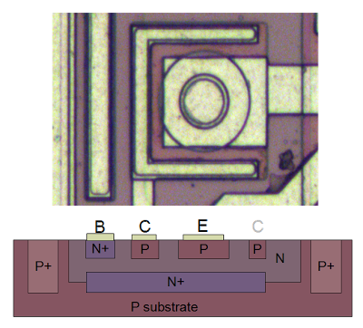
The PNP transistors have an entirely different layout from the NPN transistors. They consist of a circular emitter (P), surrounded by a ring shaped base (N), which is surrounded by the collector (P). This forms a P-N-P sandwich horizontally (laterally), unlike the vertical structure of the NPN transistors.[8]
The diagram below shows one of the PNP transistors in the TL431, along with a cross-section showing the silicon structure. Note that although the metal contact for the base is on the edge of the transistor, it is electrically connected through the N and N+ regions to its active ring in between the collector and emitter.
How resistors are implemented in silicon
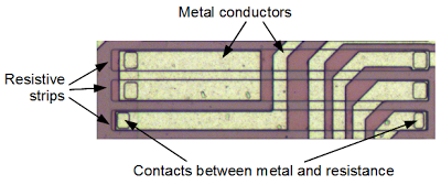
Resistors are a key component in an analog chip such as the TL431. They are implemented as a long strip of doped silicon. (In this chip, it looks like P-silicon is used for the resistors.) Different resistances are obtained by using different lengths of resistive material: the resistance is proportional to the length-to-width ratio.The photo below shows three resistors on the die. The three long horizontal strips are the resistive silicon that forms the resistors. Yellowish-white metal conductors pass over the resistors. Note the square contacts where the metal layer is connected to the resistor. The positions of these contacts control the active length of the resistor and thus the resistance. The resistance of the resistor on the bottom is slightly larger because the contacts are slightly farther apart. The top two resistors are connected in series by the metal on the upper left.
Resistors in ICs have very poor tolerance - the resistance can vary 20% from chip to chip due to variations in the manufacturing process. This is obviously a problem for a precision chip like the TL431. For this reason, the TL431 is designed so the important parameter is the ratio of resistances, especially R1, R2, R3, and R4. As long as the resistances all vary in the same ratio, their exact values don't matter too much. The second way the chip reduces the effect of variation is in the chip layout. The resistors are laid out in parallel bands of the same width to reduce the effect of any asymmetry in the silicon's resistance. The resistors are also placed close together to minimize any variation in silicon properties between different parts of the chip. Finally, the next section shows how the resistances can be adjusted before the chip is packaged, to fine-tune the chip's performance.
Silicon fuses to trim the resistors
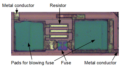
One feature of the TL431 that I didn't expect is fuses for trimming the resistances. During manufacture of the chips, these fuses can be blown to adjust the resistances to increase the accuracy of the chip. Some more expensive chips have laser-trimmed resistors, where a laser burns away part of the resistor before the chip is packaged, providing more control than a fuse.The die photo below shows one of the fuse circuits. There is a small resistor (actually two parallel resistors) in parallel with a fuse. Normally, the fuse causes the resistor to be bypassed. During manufacture, the characteristics of the chip can be measured. If more resistance is required, two probes contact the pads and apply a high current. This will blow the fuse, adding the small resistance to the circuit. Thus, the resistance in the final circuit can be slightly adjusted to improve the chip's accuracy.
Capacitors
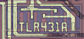
The TL431 contains two capacitors internally, and they are implemented in very different ways.The first capacitor (under the TLR431A text) is a is formed from a reverse-biased diode (the reddish and purple stripes). The junction of a reverse-biased diode has capacitance, which can be used to form a capacitor (details). One limitation of this type of capacitor is the capacitance varies with voltage because the junction width changes.
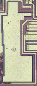
The second capacitor is formed in an entirely different manner, and is more like a traditional capacitor with two plates. There's not much to see: it has a large metal plate with the N+ silicon underneath acting as the second plate. The shape is irregular, to fit around other parts of the circuit. This capacitor takes up about 14% of the die, illustrating that capacitors use space very inefficiently in integrated circuits. The datasheet indicates these capacitors are each 20 pF; I don't know if this is the real value or not.
The TL431 chip reverse-engineered
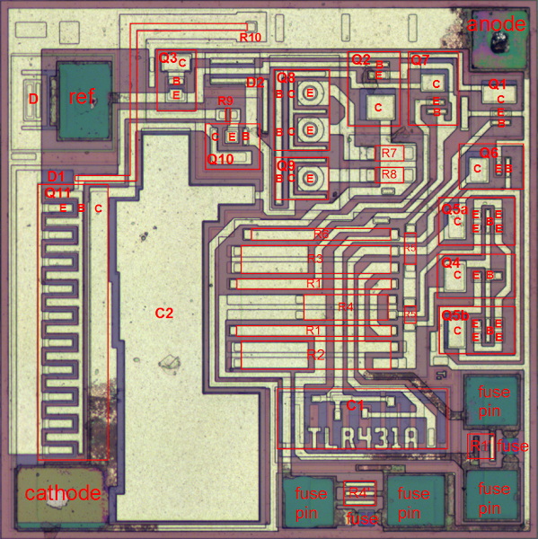
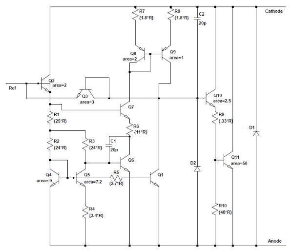
The diagram above indicates the components on the die of the TL431, labeled to correspond to the schematic below. From the earlier discussion, the structure of each component should be clear. The three pins of the chip are connected to the "ref", "anode", and "cathode" pads. The chip has a single layer of metal (yellowish-white) that connects the components. The schematic shows resistances in terms of an unknown scale factor R; 100 Ω is probably a reasonable value for R, but I don't know the exact value. One big surprise from looking at the die is the component values are very different from the values in previously-published schematics. These values fundamentally affect how the bandgap voltage reference work.[9]
How the chip works
Externally, the TL431's operation is straightforward. If the voltage on the ref pin input goes above 2.5 volts, the output transistor conducts, causing current flow between the cathode and anode pins. In a power supply, this increase in current flow signals the power supply control chip (indirectly), causing it to reduce the power which will bring the voltage back to the desired level. Thus, the power supply uses the TL431 to keep the output voltage stable.I'll give a brief summary of the chip's internal operation here, and write up a detailed explanation later. The most interesting part of the chip is the temperature-compensated bandgap voltage reference.[10] The key to this is seen by looking at the die: transistor Q5 has 8 times the emitter area as Q4, so the two transistors are affected differently by temperature. The outputs of these transistors are combined by R2, R3, and R4 in the right ratio to cancel out the effects of temperature, forming a stable reference.[11][12]
The voltages from the temperature-stabilized bandgap are sent into the comparator, which has inputs Q6 and Q1; Q8 and Q9 drive the comparator. Finally, the output of the comparator goes through Q10 to drive the output transistor Q11.
Decapping the TL431 the low tech way
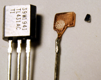
Getting an IC die photo usually involves dissolving the chip in dangerous acids and then photographing the die with an expensive metallurgical microscope. (Zeptobars describes their process here). I wondered what I'd end up with if I just smashed a TL431 open with Vise-Grip pliers and took a look with a cheap microscope. I broke the die in half in the process, but still got some interesting results. The picture below shows the large copper anode inside the package, which acts as a heat sink. Next to this is (most of ) the die, which is normally mounted on the copper anode where the white circle is. Note how much smaller the die is than the package.
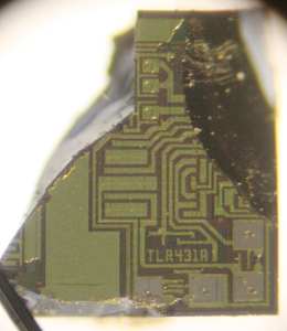
Using a basic microscope, I obtained the photo below. While the picture doesn't have the same quality as Zeptobars', it shows the structure of the chip better than I expected. This experiment shows that you can do a basic level of chip decapping and die photography without messing around with dangerous acids. From this photo I can see that the cheap TL431s I ordered off eBay are identical to the one Zeptobars decapped. Since the Zeptobars chip didn't match published schematics, I wondered if they ended up with a strange variant chip variant, but apparently not.
Conclusion
Is the TL431 really the most popular IC people haven't heard of? There's no way to know for sure, but I think it's a good candidate. Nobody seems to publish data on which ICs are produced in largest quantities. Some sources say the 555 timer is the most popular chip with a billion produced every year (which seems improbably high to me). The TL431 must be high up the popularity list - you probably have a TL431 within arms-reach right now (in your phone charger, laptop power adapter, PC power supply, or monitor). The difference is that chips such as the 555 and 741 are so well-known that they are almost part of pop culture with books, T-shirts and even mugs. But unless you've worked on power supplies, chances are you've never heard of the TL431. Thus, the TL431 gets my vote for the most common IC that people are unaware of. If you have other suggestions for ICs that don't get the attention they deserve, leave a comment.Acknowledgments
The die photos are by Zeptobars (except the photo I took). The schematic and analysis are heavily based on Cristophe Basso's work.[12] The analysis benefited from discussion with Mikhail of Zeptobars, and the Visual 6502 group, in particular B. Engl.Notes and references
[1] Because the TL431 has an unusual function, there's no standard name for its function. Different datasheets describe it as a "adjustable shunt regulator", a "programmable precision reference", a "programmable shunt voltage reference", and a "programmable zener".
[2] I dug up some history on the origins of the TL431 from Texas Instruments' Voltage Regulator Handbook (1977). The precursor chip, the TL430, was introduced as an adjustable shunt regulator in 1976 The TL431 was created as an improvement to TL430 with better accuracy and stability and was called a precision adjustable shunt regulator. The TL431 was announced as a future product in 1977 and launched in 1978. Another future product that TI announced in 1977 was the TL432, which was going to be "Timer/Regulator/Comparator Building Blocks", containing a voltage reference, comparator, and booster transistor in one package. preliminary datasheet. But when the TL432 came out, the "building block" plan had been abandoned. The TL432 ended up being merely a TL431 with the pins in a different order, to help PC board layout. datasheet.
[3] Modern ATX power supplies (example, example) often contain three TL431s. One provides feedback for the standby power supply, another provides feedback for the main power supply, and a third is used as a linear regulator for the 3.3V output.
[4] It's interesting to look at the switching power supplies that don't use the TL431. Earlier switching power supplies typically used a Zener diode as a voltage reference. The earliest Apple II power supplies used a Zener diode as the voltage reference (Astec AA11040), but this was soon replaced by a TL431 in the Astec AA11040-B revision. The Commodore CBM-II model B used a TL430 instead of TL431, which is an unusual choice. HP-1000 minicomputers used both the TL430 (p69) and the TL431 (p73). The original IBM PC power supply used a Zener diode for reference (along with many op amps). Later PC power supplies often used the TL494 PWM controller, which contained its own voltage reference and operated on the secondary side. Other ATX power supplies used the SG6105 which included two TL431s internally.
Phone chargers usually use the TL431. Inexpensive knockoffs are an exception; they often use a Zener diode instead to save a few cents. Another exception is chargers such as the iPad charger, which use primary-side regulation and don't use any voltage feedback from the output at all. See my article on power supply history for more information.
[5] The TL431 is available in a larger variety of packages than I'd expect. Two of the photos show the TL431 in a transistor-like package with three leads (TO-92). The remaining photos show the surface-mounted SOT23-3 package. The TL431 also comes in 4-pin, 5-pin, 6-pin, or 8-pin surface-mounted packages (SOT-89, SOT23-5, SOT323-6, SO-8 or MSOP-8), as well as a larger package like a power transistor (TO-252) or an 8-pin IC package (DIP-8). (pictures).
[6] For more information on how bipolar transistors are implemented in silicon, there are many sources. Semiconductor Technology gives a good overview of NPN transistor construction. Basic Integrated Circuit Processing is a presentation that describes transistor fabrication in great detail. The Wikipedia diagram is also useful.
[7] You might have wondered why there is a distinction between the collector and emitter of a transistor, when the simple picture of a transistor is totally symmetrical. Both connect to an N layer, so why does it matter? As you can see from the die photo, the collector and emitter are very different in a real transistor. In addition to the very large size difference, the silicon doping is different. The result is a transistor will have poor gain if the collector and emitter are swapped.
[8] The PNP transistors in the TL431 have a circular structure that gives them a very different appearance from the NPN transistors. The circular structure used for PNP transistors in the TL431 is illustrated in Designing Analog Chips by Hans Camenzind, who was the designer of the 555 timer. If you want to know more about analog chips work, I strongly recommend Camenzind's book, which explains analog circuits in detail with a minimum of mathematics. Download the free PDF or get the printed version.
The structure of a PNP transistor is also explained in Principles of Semiconductor Devices. Analysis and Design of Analog Integrated Circuits provides detailed models of bipolar transistors and how they are fabricated in ICs.
[9] The transistors and resistors in the die I examined have very different values from values others have published. These values fundamentally affect the operation of the bandgap voltage reference. Specifically, previous schematics show R2 and R3 in a 1:3 ratio, and Q5 has 2 times the emitter area as Q4. Looking at the die photo, R2 and R3 are equal, and Q5 has 8 times the emitter area as Q4. These ratios result in a different ΔVbe. To compensate for this, R1 and R4 are different between previous schematics and the die photo. I will explain this in detail in a later article, but to summarize Vref = 2*Vbe + (2*R1+R2)/R4 * ΔVbe, which works out to about 2.5 volts. Note that the ratio of the resistances matters, not the values; this helps counteract the poor resistor tolerances in a chip.
In the die, Q8 is formed from two transistors in parallel. I would expect Q8 and Q9 to be identical to form a balanced comparator, so I don't understand the motivation behind this. My leading theory is this adjusts the reference voltage up slightly to hit 2.5V. B. Engl suggests this may help the device operate better at low voltage.
[10] I won't go into the details of a bandgap reference here, except to mention that it sounds like some crazy quantum device, but it's really just a couple transistors. For more information on how a bandgap reference works, see How to make a bandgap voltage reference in one easy lesson by Paul Brokaw, inventor of the Brokaw bandgap reference. A presentation on the bandgap reference is here.
[11] In a sense, the bandgap circuit in the TL431 operates "backwards" to a regular bandgap voltage reference. A normal bandgap circuit provides the necessary emitter voltages to produce the desired voltage as output. The TL431's circuit takes the reference voltage as input, and the emitter voltages are used as outputs to the comparator. In other words, contrary to the block diagram, there is not a stable voltage reference inside the TL431 that is compared to the ref input. Instead, the ref input generates two signals to the comparator that match when the input is 2.5 volts.
[12] There are many articles about the TL431, but they tend to be very technical, expecting a background in control theory, Bode plots, etc. The TL431 in Switch-Mode Power Supplies loops is a classic TL431 paper by Christophe Basso and Petr Kadanka. This explains the TL431 from the internals through loop compensation to an actual power supply. It includes a detailed schematic and description of how the TL431 operates internally. Other related articles are at powerelectronics.com. Designing with the TL431, Ray Ridley, Switching Power Magazine is a detailed explanation of how to use the TL431 for power supply feedback, and the details of loop compensation. The TL431 in the Control of Switching Power Supplies is a detailed presentation from ON Semiconductor. The TL431 datasheet includes a schematic of the chip's internals. Strangely, the resistances on this schematic are very different from what can be seen from the die.
18 comments:
thanks
shared with
https://plus.google.com/u/0/communities/105266405842890740625
Interesting read. Thanks for taking the time to write these posts, they seem well researched and I imagine there are quite a few hours in each of them.
As of your suggestion I put a very small donation ($5) towards your daughters school water charity.
/Markus
Surprisingly fewer comments here than I would have thought. Thanks for this post -- I learned something new about how transistors, resistors and capacitors are implemented in silicon.
Great post! As someone who is trying to learn electronics on their own it's a really excellent lesson to have the veil lifted on these tiny things.
Well thought out and well written too. I hope you feel inspired to keep delivering :-)
French guy: I can't identify your chip, but my guess is a NEC (now Renesas) microcontroller, probably custom. Lots of foreign sites offer to sell a NEC 800279F1-011-MN9 (i.e. the chip you're looking at), but nobody says what it is so they're probably bluffing.
Analyzing your chip would be very hard - you'd need to start stripping off the metal layers and look at what's underneath. P.S. The image site you use tries to download some dodgy files.
Thank you for the effort to put toghether all this info, and i subscribe at your ideea about 431 being the most illustre unknown ic at the moment.
Great information!. Just for interest I built a reflex-regenerative medium wave receiver using only a TL431 device as its active component. It is a great performer.
http://theradioboard.com/rb/viewtopic.php?f=4&t=6733
Great post, superb. I learned a lot and appreciate your time spent writing this article.
Thanks
/Luis
Fantastic, Really appreciate the effort and time you have spent. I look into the die details for TL431 size and find links
1. https://zeptobars.com/en/read/TL431-adjustable-shunt-regulator-linear-supply and
2. https://zeptobars.com/en/read/TI-TL431-adjustable-shunt-regulator-linear-supply
Why the area is different ? is it just because manufacturer different ?
Thanks
Sunil: yes, different manufacturers use different layouts and often different circuits. The part number doesn't mean much - internally two TL431s (or 741 op amps or whatever) can be very different. So read the data sheet carefully :-)
It is worth it to mention that (at least in the SMD land) that pinout varies a lot among manufactures, all under the same package format and "TL431" or "431" label. I know it well after spending some time trying to make one of these working. Awesome investigative pages here in this blog, congratulations and thanks!!
Thanks man for this detailed explanation of the de-capped IC. I have a decapped linear regulator controller IC and was unable to make sense of it. The references in your post have been highly useful. Keep up the good work
Must have a lot of time on your hands. Perhaps next time, use it to cure some deadly disease, alleviate world hunger, stop global warming, reduce micro-plastics, invent time travel...
Hi Ken, have you tried your TL431 circuit in SPICE to see if it's results match the datasheets? If so then what where the SPICE device parameters used for the transistors, etc? Thanks.
After reading this blog, I learned that the original TL431 chip could be used in multiple components. I just thought that this chip was widely used before, but it's still not very systematic to understand which scenarios it's applied to. Thanks to the author, let me know that the whole TL431 chip can be re-engineered with transistors, resistors, fuses and capacitors.
And I'm very amazed at the details of your photos. Particularly when I saw that you marked the structure of the TL431 chip component in detail on the picture and matched the internal schematic diagram of the TL431 that you provided, it seemed to make me feel that there is an amiable teacher behind the screen who is patient, Teach the reader gently.
So I am very happy to come across such an illuminating article, and I very much agree with this view, "And I'm very amazed at the details of your photos. Particularly when I saw that you marked the structure of the TL431 chip component in detail on the picture and matched the internal schematic diagram of the TL431 that you provided, it seemed to make me feel that there is an amiable teacher behind the screen who is patient, Teach the reader gently.
So I am very happy to come across such an illuminating article, and I very much agree with this view, "But unless you've worked on power supplies, chances are you've never heard of the TL431. Thus, the TL431 gets my vote for the most common IC that people are unaware of."
And I also write an article about how to test and replace tl431, hope it can be insightful to you.
https://www.apogeeweb.net/circuitry/tl431-test-and-repalce.html
Excellent post!
I wrote some analysis and simulation about TL431, including a basic analysis of the schematic from your reverse-engineering: https://chenshuo.github.io/notes/tl431/#another-schematic-by-ken-shirriff
Let me know if I missed anything interesting. Thanks.
The URL for the article on "How to Make a bandgap voltage reference in one easy lesson" has changed. It is now:
https://www.renesas.com/us/en/document/whp/how-make-bandgap-voltage-reference-one-easy-lesson-paul-brokaw
I found it via a Google search for the title. Hope this helps other readers.
Post a Comment