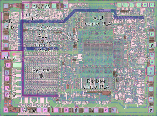
The photograph below is a highly magnified image of the 8085's silicon, showing the relevant parts of the chip. In the upper-left, the arithmetic logic unit (ALU) performs 8-bit arithmetic operations. The status flag circuitry is below the ALU and the flags are connected to the data bus (indicated in blue). To the right of the ALU, the control PLA decodes the instructions into control lines that control the operations of the ALU and flag circuits.
The 8085 has seven status flags.- Bit 7 is the sign flag, indicating a negative two's-complement value, which is simply a byte with the top bit set.
- Bit 6 is the zero flag, indicating a value that is all zeros.
- Bit 5 is the undocumented K (or X5) flag, indicating either a carry from the 16-bit incrementer/decrementer or the result of a signed comparison. See my article on the undocumented K and V flags.
- Bit 4 is the auxiliary carry, indicating a carry out of the 4 low-order bits. This is typically used for BCD (binary-coded decimal) arithmetic.
- Bit 3 is unused and set to 0. Interestingly, a fairly large transistor drives the data bus line to 0 when reading the flags, so this unused flag bit doesn't come for free.
- Bit 2 is the parity flag, which is set if the result has an even number of 1 bits.
- Bit 1 is the undocumented signed overflow flag V (details).
- Bit 0 is the carry flag.
The image below zooms in on the flag silicon, showing individual transistors. The large transistors labeled with the flag name drive the flag value onto the data bus. From the data bus, the flag values control the results of conditional jumps, calls, and returns. The complex circuits above these transistors compute and store the flag values.
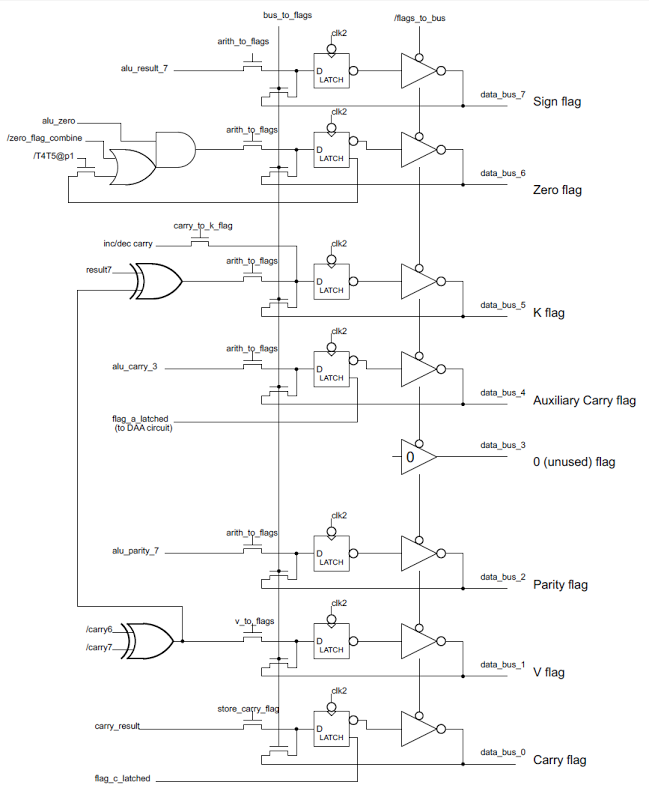
The schematic below shows the flag circuit that is implemented in the silicon above.
Each flag bit has a latch and control lines to write a value to the latch. Most flags are updated by the same arithmetic instructions and controlled by the arith_to_flags control line. The carry flag is affected by additional instructions and has its own control line. The undocumented K and V flags are updated in different circumstances and have their own control lines.
The bus_to_flags control loads the flags from the data bus for the POP PSW instruction, while the flags_to_bus control sends the flag values over the data bus for the PUSH PSW instruction or for conditional branches.
The circuitry to compute most flag values is straightforward. The sign flag is set based on bit 7 of the result. The auxiliary carry flag is set on the carry out of bit 3. The K and V flags are set based on the top two bits (details).
The zero flag is normally set from the alu_zero signal that indicates all bits are zero.
The zero flag has support for multi-byte zero: at each step it can AND the existing zero flag with the current ALU zero value, so the zero flag will be set if both bytes are zero. This is only used for the (undocumented) DSUB 16-bit subtract instruction. Strangely, this circuit is also activated for the 16-bit DAD instructions, but the result is not stored in the flag.
If you look at the chip photograph at the top of the article, the flags are arranged in apparently-random order, not in their bit order as you might expect. Presumably the layout used is more efficient. Also notice that the carry flag C is off to the right of the ALU. Because of the complexity of the carry logic, which will be discussed next, the circuitry wouldn't fit under the ALU with the rest of the flag logic.
The carry logic
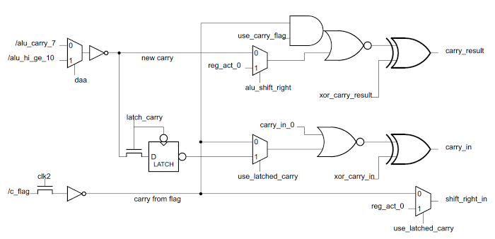
The schematic below shows the circuit for the carry flag. The logic for carry is more complex than for the other flags because carry is used in a variety of ways.
The value stored in the carry flag
The top part of the circuit computescarry_result, the value stored in the carry flag.
This value has several different meanings depending on the instruction:
- For arithmetic operations, the carry flag is loaded with the value generated by the ALU. That is,
alu_carry_7(the high-order carry from bit 7 of the ALU) is used. (See Inside the ALU of the 8085 microprocessor for details on how this is computed.) - For
DAA(decimal adjust accumulator), the carry flag is set if the high-order digit is >= 10. This value isalu_hi_ge_10, which is selected by thedaacontrol line. - For
CMC(complement carry), the carry flag value is complemented. To compute this, the previous carry flag valuec_flagis selected byuse_carry_flagand complemented by thexor_carry_resultcontrol line. - For
ARHL/RAR/RRC(rotate right operations), bit 0 of the rotated value goes into the carry. In the circuit,reg_act_0(the low-order bit in the undocumented ACT (accumulator temp) register) is selected by thealu_shift_rightcontrol line.
xor_carry_result control inverts the carry value in a few cases. For subtraction and comparison, it flips the carry bit to be the borrow bit. For STC (set carry), the xor_carry_result control forces the carry to 1. For AND operations, it forces the carry to 0.
Generating the carry input signal
The middle part of the circuit selects the appropriatecarry_in value that is supplied to the ALU.
carry_in_0 and optionally xor_carry_in. This is used for most instructions.
xor_carry_in control does this.
LDHI and LDSI instructions.
These instructions add a constant to a 16-bit register pair, so they need to add the carry from of the low-order sum to the high-order byte. The carry latch temporarily holds the carry, and this value is selected by the use_latched_carry control line. You might wonder why not just use the normal carry flag; the LDHI and LDSI instructions are designed to leave the carry flag unchanged, so they need somewhere else to temporarily store the carry.
The surprising conclusion that Intel deliberately included circuitry in the 8085 specifically to support these undocumented instructions, and then decided not to support these instructions. (In contrast, the 6502's unsupported instructions are just random consequences of unsupported opcodes.)
Generating the shift_right input signal
Each bit of the ALU has a shift right input. For most of the bits, the input comes from the bit to the left, but the high-order bit uses different inputs depending on the instruction. The bottom circuit in the schematic below generates the shift right input for the ALU. This circuit has two simple options.- Normally the carry flag is fed into
shift_right_in. For theARHLandRARinstructions, this causes the carry flag to go into the high-order bit. - For the
RRCandRLCinstructions (rotate A left/right), therotate_carrycontrol selects bit 0 as the shift right input.
Conclusions
By reverse-engineering the 8085, we can see how the flag circuits in the 8085 actually works at the gate and silicon level. One interesting feature is the circuitry to implement undocumented instructions and flags. Another interesting feature is the complexity of the carry flag compared to the other flags.This information is based on the 8085 reverse-engineering done by the visual 6502 team. This team dissolves chips in acid to remove the packaging and then takes many close-up photographs of the die inside. Pavel Zima converted these photographs into mask layer images, generated a transistor net from the layers, and wrote a transistor-level 8085 simulator.
Footnotes on rotate
I recommend you skip this section, but there are few confusing things about the rotate logic that I wanted to write down.
For some reason the rotate operations are named very strangely in the 8080 and 8085. RRC is the "rotate accumulator right" instruction and RAR is the "rotate accumulator right through carry" instruction. Based on the abbreviations, the names seem reversed. The left rotates RLC and RAL are similar. The Z-80 processor has a similar RRC instruction, but calls it "rotate right circular", making the abbreviation slightly less nonsensical.
Bit 0 of ACT is fed into shift_right_in for both RRC and RLC.
However, this input is just ignored for RLC since the rotation is the other direction, so I assume this is just a result of the control logic treating RRC and RLC the same.)
To reduce the control circuitry, the rotate_carry and use_latched_carry control lines are actually the same control line since the instructions that use them don't conflict. In other words, there is just one control line, but it has two distinct functions.


Cool. Didn't know anybody cared about 8085's anymore. I started my career writing firmware in assembly language for scientific instruments based on 8085. We only had 8K ROM on the low end systems, but I was able to shoehorn enough code to run the display and touchpanel input, control the sensors and data acquisition, and provide RS232 and parallel I/O, etc. I think I still have some of my old tricks, including some pretty good math subroutines, even a log approximation I used to generate the logarithmic display.
ReplyDeletePlease remember to tag this article with 8085. I love your other 8085 articles (esp. the ALU one) and I'd love to be able to see them all by just bookmarking the 8085 label.
ReplyDeleteThis is fantastic. I love to see this level of analysis and reverse engineering!
ReplyDeleteThere are 7 flags out of which only 5 are accessible :
ReplyDeleteb7 b6 b5 b4 b3 b2 b1 b0
S Z - AC - P - CY
then my question is that among the flags b4 to b7 can the value be A hex.(ie 10 in decimal, bcoz the flag b5 is always 0 and in number 10 b5 should be set to 1)....
By the way, my flag register has a value of A6.