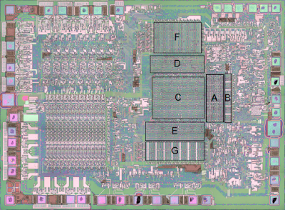
The following diagram shows the arrangement of the PLA on the chip (image from Visual 6502). The PLA has 5 planes, which I have labeled A through G.
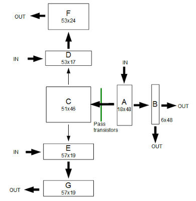
The block diagram below shows approximately how the planes are connected. Plane A receives inputs from the instruction circuit. Its outputs are fed into the small plane B, producing outputs that go into the instruction circuit. The outputs from A also are fed into C (through pass transistors).
Planes D and E can be considered the same plane, split apart for better layout. They share 11 input lines, and the remaining inputs are different between D and E. These inputs come from the ALU/register circuits on the left, as well as other parts of the chip. They also receive inputs from G - these inputs are not handled via normal PLA input lines, but are wired through transistors directly to the associated output lines, which makes the layout more compact.
Planes F and G provide outputs through pass transistors to the ALU/register circuits. These outputs probably control the actions and bus activity, but more analysis is needed.
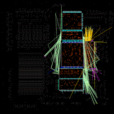
The following diagram shows how the PLA planes are wired to the rest of the chip. Planes D and E in particular receive inputs from many parts of the chip. The outputs from F and G are very short because the displayed wires end at the nearby pass transistors to the left.
The transistors in the PLA
I have diagrams showing where the transistors are in each PLA grid here.


2 comments:
Great - thanks for putting this out on public display!
nice stuff
keep it up :)
you can also follow my site about microprocessor
http://microprocessorforyou.blogspot.com
Post a Comment