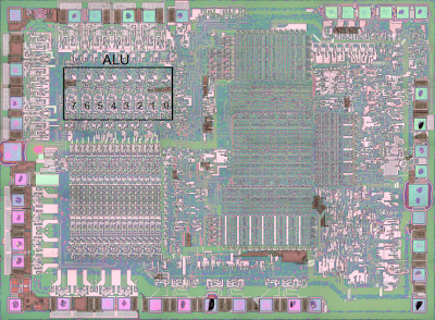
The following diagram shows the location of the ALU in the 8085. The ALU is 8 bits wide, with the high-order bit on the left. The register file is the large block below the ALU. The registers are 16 bits wide, made up of pairs of 8-bit registers. Surprisingly, the register file has the high-order bit on the right, the opposite order from the ALU.
The ALU takes two 8-bit inputs, which I'll call A and X, and performs one of five basic operations: ADD, OR, XOR, AND, and SHIFT-RIGHT. As well, if the input X is inverted, the ALU can perform subtraction and complement operations. You might think SHIFT-LEFT is missing from this list. However, it is simply performed by adding the number to itself, which shifts it to the left one bit in binary. Note that the 8085 arithmetic operations are very basic. There is no multiplication or division operation - these were added in the 8086.
The ALU consists of 8 mostly-identical slices, one for each bit. For addition, each slice of the ALU adds the appropriate input bits, computing the sum A + X + carry-in, generating a sum bit and a carry-out bit. That is, each bit of the ALU implements a full adder. The logic operations simply operate on the two input bits: A AND X, A OR X, A XOR X. Shift-right simply outputs the A bit from the slice to the right.
ALU schematic
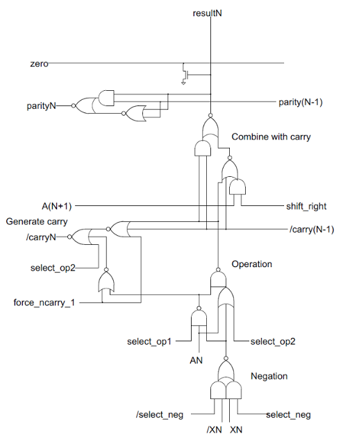
The following schematic shows one bit of the ALU. The schematic has roughly the same layout as the implementation on the chip, flowing from bottom to top. Eight of these circuits are stacked side-by-side, with the low-order bit on the right. Carries flow from right to left, and bits shifted right flow from left to right.Negation
Starting at the bottom of the schematic, is the complex gate labeled Negation. This gate optionally selects a negated second argument by selecting either XN or /XN. (XN is the Nth bit of the second argument, which I'll call X. The / indicates the complement.) For most of the discussion below I'll assume XN is uncomplemented to keep things simpler.Operation
Above the complement selector are a few gates labeled Operation that perform the desired 2-input operation. The NAND gate on the left generates either A NAND X or 1 based on the select_op1 control line. The OR gate on the right generates either A OR X or 1, based on the select_op2 control line. Combining these in the NAND gate yields four different possibilities:| select_op1 | select_op2 | Result |
|---|---|---|
| 0 | 0 | A NOR X |
| 0 | 1 | 0 |
| 1 | 0 | A NXOR X |
| 1 | 1 | A AND X |
Combine with carry
Above the operation circuit is the next block of gates labeled Combine with carry that generates the ALU output by merging the carry-in with the operation value via XOR.To understand this circuit, first consider the following simple XOR circuit, which is used a couple times in the ALU. It can be understood fairly simply: if both inputs are 0 (top) or both inputs are 1 (bottom) then the output is 0.
Ignoring the shift_right circuit for a moment, the block of gates is simply the XOR circuit above. Note that XOR with 0 is a no-op, while XOR with 1 complements the value. And A XOR X XOR CARRY is the low-order bit of adding A, X, and CARRY.
The key point of this circuit is that the incoming carry is generated with the proper value to convert the operation output into the desired final result. The incoming carry /carry(N-1) is either 0, 1, or the complemented carry from bit N-1 as appropriate.
| Op | Operation output | Carry | Result |
|---|---|---|---|
| or | A NOR X | 1 | A OR X |
| add | A NXOR X | /carry | A XOR X XOR CARRY |
| xor | A NXOR X | 1 | A XOR X |
| and | A AND X | 0 | A AND X |
| shift right | 0 | 0 | A(N+1) |
| complement | A NOR /X | 1 | A OR /X |
| subtract | A NXOR /X | /carry | A XOR /X XOR CARRY |
Note that the carry-in line must have the right value in order to generate the appropriate output. For addition it passes the inverted carry from one bit to the next. But for OR, XOR, the line is set to 1. And for AND and SHIFT_RIGHT it is set to 0. As will be seen below, the carry circuitry generates the right value for the right operation.
The final aspect of this circuit is the shift-right circuit. With a 0 op input, 0 carry input, and shift_right set, the output is simply the bit from the right: A(N+1).
Generate carry
The circuit on the left, labeled Generate carry generates the carry out. It can generate three different outputs: 1, 0, or the (complemented) carry from the sum. If select_op2 is set, it will force the carry to 0. Otherwise if force_ncarry_1 is set, it will force the carry to 1. Otherwise, the carry is generated for the sum of A + X + carry-in through straightforward logic: If the carry-in is set, and one of the inputs is set, there will be a carry out. If both input bits are set, there will be a carry out.Flags
The 8085 has a parity flag, which is 1 if the number of 1 bits is even, and 0 if the number of parity bits is odd. The parity flag is generated by XORing all the result bits together (and complementing). Each bit is XORed with the lower-order parity value by the parity circuit near the top of the schematic. The XOR circuit is the same circuit described above.The zero flag is computed by a simple circuit: each result bit drives a transistor that will pull the zero line low if the bit is set. This forms an 8-input NOR gate, spread across the ALU.
The control lines
As seen in the schematic, the 8085 uses multiple control lines to control the activity inside the ALU. In total, the ALU provides 7 different operations and the following table summarizes the control lines that are used for each operation. It also lists the opcodes that use each ALU operation.
| Operation | select_neg | select_op1 | select_op2 | shift_right | force_ncarry_1 | Opcodes |
|---|---|---|---|---|---|---|
| or | 0 | 0 | 0 | 0 | 1 | ORA,ORI (and default) |
| add | 0 | 1 | 0 | 0 | 0 | INR,DCR,RLC,DAD,RAL,DAA,ADD,ADC,ADI,ACI (and undocumented LDSI,LDHI,RDEL) |
| xor | 0 | 1 | 0 | 0 | 1 | XRA,XRI |
| and | 0 | 1 | 1 | 0 | 1 | ANA,ANI |
| shift right | 0 | 0 | 1 | 1 | 1 | RRC,RAR (ARHL) |
| complement | 1 | 0 | 0 | 0 | 1 | CMA |
| subtract | 1 | 1 | 0 | 0 | 0 | SUB,SBB,SUI,SBI,CMP,CPI (DSUB) |
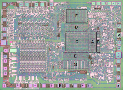
The ALU control lines are generated from the opcode by the programmable logic array. Specifically, they are outputs from PLA F, which is to the right of the ALU. More details are in my article on the PLA. The ALU has additional control lines to set up the registers, initialize the carry bits, and set the flags. These control the differences between different op codes, beyond the categories above. the I will explain those in a future article.
Reverse-engineering the ALU
This information is based on the 8085 reverse-engineering done by the visual 6502 team. This team dissolves chips in acid to remove the packaging and then takes many close-up photographs of the die inside. Pavel Zima converted these photographs into mask layer images, generated a transistor net from the layers, and wrote a transistor-level 8085 simulator.I took the transistor net and used it to figure out how the ALU works. First, I converted the transistor net into gates. Next I figured out which gates are part of the ALU and put them into a schematic. Then I examined how the circuit worked for different operations and eventually figured out how it works.
Conclusion
The ALU of the 8085 is an interesting circuit. At first it seemed like an incomprehensible pile of gates with mysterious control lines, but after some investigation I figured it out. The 8085 ALU is implemented very differently from the 6502's ALU (which I'll write up later). The 6502's ALU uses fairly straightforward circuits to generate the SUM, AND, XOR, OR, and SHIFT values in parallel, and then uses a simple pass-transistor multiplexor to pick the desired operation. This is in contrast to the 8085 ALU, which generates only the desired value.


Excellent post! I've reposted it to Retro Communities at https://plus.google.com/communities/109052413018437647853
ReplyDeleteOkay, now i understand the reason why the 6502 has illegal opcodes that combine 2 alu commands with each other....
ReplyDeleteAnonymous: if you want to know the details of 6502 illegal opcodes, the page to read is pagetable.com.
ReplyDeleteIt is interesting, how value for /XN input is generated. Is there one more adder for that?
ReplyDeleteAnonymous: I should have given XN and /XN the names TMPN and /TMPN: they come from the TMP register, which holds one of the arguments for the ALU. Since each latch in TMP is a pair of inverters, the complemented bit is available "for free".
ReplyDeleteKen this is great information. Have a question from my students, why during AND operation AC is set? Could not get a very good answer, can you help please? Thanks a lot. from Prad
ReplyDeleteHi Prad. That's a great question, which AC gets set during an AND operation.
ReplyDeleteThere are two factors. First, the Sign, Zero, Auxiliary Carry, and Parity flags are all loaded by the same control line, for arithmetic instructions. Thus, the AC flag gets set to something for AND instructions, even though it doesn't make a lot of sense.
Second, the ALU circuit happens to output 0 on the internal inverted-carry line for an AND instruction. (See the table under "Combine with Carry" above.) This 0 is just the value the ALU circuit generates for AND. For OR, it happens to generate 1. Remember that these are inverted values.
Putting these two factors together, the AC flag is set for AND operations and cleared for OR operations. This doesn't really make mathematical sense; it's just a consequence of how the circuit is implemented.
I'm planning to write another blog post about the ALU and flags, so I'm interested in the questions people have.
Ken Thanks a lot for the answer given. I will check for other instructions also which have flags reset or set but not in a very logical way. In the mean time thanks again and information you have put here is very nice indeed. From Prad
ReplyDeleteCan you show the reverse engineering of pic16f84 mcu.Thanks in adv...
ReplyDeleteShift-right simply outputs the A bit from the slice to the right.
ReplyDeleteYou mean from the left.
Hey ken, where is this carry is coming from ? Is this the carry which generates from sum operation? Why there is a circuit for generation of carry? I have a lot of confusion regarding from carry concept?
ReplyDeleteAnonymous: when you add two binary bits, you get a sum bit and a carry bit. E.g. 1 + 1 = carry 1, sum 0. See Full Adder for more details.
ReplyDelete